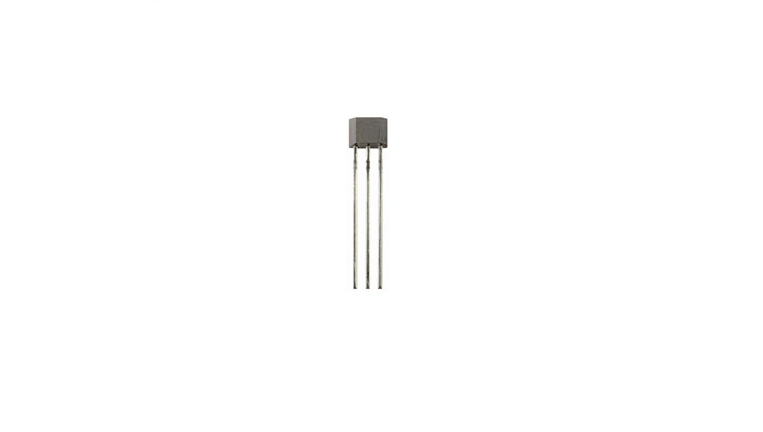
Honeywell Digital Position Sensor ICs SS41K6 Installation Guide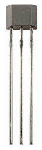
GENERAL INFORMATION
CAUTIONELECTROSTATIC DISCHARGE DAMAGEEnsure proper ESD precautions are followed when handling this product.Failure to comply with these instructions may result in product damage.
SOLDERING AND ASSEMBLY
CAUTIONIMPROPER SOLDERING
- Ensure leads are adequately supported during any forming/shearing operation so that they are not stressed inside the plastic case.
- Limit exposure to high temperatures. Failure to comply with these instructions may result in product damage
Wave solder at 250°C to 260°C [482°F to 500°F] for a maximum of three seconds. Burrs are allowed only if full lead length will pass through a 0,68 mm [0.027 in] dia. hole.
CLEANING
CAUTIONIMPROPER CLEANINGDo not use pressure wash. High-pressure stream could force contaminants into the package.Failure to comply with these instructions may result in product damage.Use agitated rinse to clean the sensor.
Performance Specifications (At VS = 4.5 V to 60 V, TA = -40ºC to 150ºC [-40ºF to 302ºF], IO = 15 mA, except where otherwise specified.)
| Characteristic | Symbol | Condition | Min. | Typ. | Max. | Unit |
|
Supply voltage |
VS | — | 4.5 | — | 60.0 |
V |
| -40ºC to 125ºC [-40ºF to 257ºF] | 4.5 | — | 60.0 | |||
| 150ºC [302ºF] | 4.5 | — | 24.0 | |||
| Supply current | IS | — | — | 3.6 | 10.0 | mA |
| Output voltage (ON) | VSAT | IO = 15 mA | — | 0.215 | 0.600 | V |
| Output leakage current | IOH | — | — | — | 10.0 | mA |
| Output current limit1 | IO(SCP) | short circuit protection1 | 40 | — | — | mA |
| Output switching time: |
ms |
|||||
| rise time | tr | TA = 25ºC [77ºF] | — | — | 1.5 | |
| fall time | tf | TA = 25ºC [77ºF] | — | — | 1.5 | |
| ESD (Human Body Model) | VESD | per JEDEC JS-001-2014 | -16 | — | 16 | kV |
| Operating temperature | TA | — | -40 [-40] | — | 150 [302] | ºC [ºF] |
| Junction temperature | TJ | — | -40 [-40] | — | 165 [329] | ºC [ºF] |
| Storage temperature | TS | — | -40 [-40] | — | 150 [302] | ºC [ºF] |
| Thermal resistance | RqJA | — | — | — | 233 | ºC/W |
| Soldering time and temperature | — | 3 s max. | 250 [482] | — | 260 [500] | ºC [ºF] |
NOTICE
These Hall-effect sensor ICs may have an initial output in either the ON or OFF state if powered up with an applied magnetic field in the differential zone (applied magnetic field >BRP and <BOP). Honeywell recommends allowing 10 µs after the supply voltage has reached 4.5 V for the output voltage to stabilize.
NOTICE
The magnetic field strength (Gauss) required to cause the switch to change state (operate and release) will be as specified in the magnetic characteristics (see Table 2). To test the switch against the specified limits, the switch must be placed in a uniform magnetic field.
Bipolar Hall-Effect Digital Position Sensor ICs
Magnetic Characteristics (At VS = 4.5 V to 60 V, TA = -40ºC to 150ºC [-40ºF to 302ºF], except where otherwise specified.)
| Characteristic | Symbol | Condition | Min. | Typ. | Max. | Unit |
| Operate | BOP | —
TA = 25ºC [75ºF] |
—
— |
25
25 |
115
65 |
Gauss |
| Release | BRP | —
TA = 25ºC [75ºF] |
-115
-65 |
-25
-25 |
—
— |
Gauss |
| Differential | BDIF | — | 30 | — | — | Gauss |
Absolute Maximum Specifications
| Characteristic | Symbol | Condition | Min. | Typ. | Max. | Unit | |||||||||||||||||||||||||||||||||||
| Supply voltage | Vs | — | -0.5 | — | 60.0 | V | |||||||||||||||||||||||||||||||||||
| Output voltage | VO | — | -0.5 | — | 60.0 | V | |||||||||||||||||||||||||||||||||||
| Output current | IO | — | — | — | N/A1 | mA | |||||||||||||||||||||||||||||||||||
| Magnetic flux | B | — | — | — | no limit | Gauss
|
Output short circuit protection is enabled when the output load current exceeds the rated load current shown in Table 1
NOTICEAbsolute maximum ratings are the extreme limits the device will momentarily withstand without damage to the device. Electrical and mechanical characteristics are not guaranteed if the rated voltage and/or currents are exceeded, nor will the device necessarily operate at absolute maximum ratings.
Magnetic Characteristics vs Temperature
References
[xyz-ips snippet=”download-snippet”]