![]() Voltage Controlled FilterV3320
Voltage Controlled FilterV3320
Overview
The V3320 is a high-performance voltage-controlled four-pole filter with voltage controllable resonance. A wide variety of filter responses, such as low pass, high pass, bandpass, and all pass can be achieved by connecting the four independent sections. A single input exponentially controls the frequency over greater than a ten-octave range with little control voltage feed-through. Another input controls the resonance from zero to low distortion oscillation in a manner of modified linearity.Every filter section includes a novel variable gain cell and a buffer. The variable gain cell features a better signal-to-noise ratio and low distortion.
Features
- ±15V Volt Supplies
- Low Cost
- Voltage Controllable Frequency: 12-octave range minimum
- Accurate Exponential Frequency Scale
- Accurate Linear Resonance Scale
- Low Control Voltage Feedthrough: -45 dB typical
- Filter Configurable into the low pass, high pass, all pass, etc
- Large Output: .12 V.P.P. typical
- Low Noise: -86dB typical
- Low Distortion in Passband: 0.1% typical
- Low Warm-Up Drift
- Configurable into Low Distortion Voltage Controlled Sine Wave Oscillator
Pin configuration
 |
SOP18L | |
| IN1 | 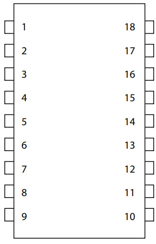 |
IN4 |
| IN2 | IN3 | |
| GND | OUT3 | |
| OUT2 | BOUT3 | |
| OUT1 | VCC | |
| BOUT2 | VSS | |
| BOUT1 | FCIN | |
| GM-IN | OUT4 | |
| RCIN | BOUT4 |
Typical Applications
- Voltage Controlled Filter
PIN Description
| No. | Name | Functions Description | No. | Name | Functions Description |
| 1 | IN1 | First Gain Cell Input | 10 | BOUT4 | Fourth Buffer Output |
| 2 | IN2 | Second Gain Cell Input | 11 | OUT4 | Fourth Gain Cell Output |
| 3 | GND | GND | 12 | FCIN | Frequency Cntl Input |
| 4 | OUT2 | Second Gain Cell Output | 13 | VSS | Negative Voltage |
| 5 | OUT1 | First Gain Cell Output | 14 | VCC | Positive Voltage |
| 6 | BOUT2 | Second Buffer Output | 15 | BOUT3 | Third Buffer Output |
| 7 | BOUT1 | First Buffer Output | 16 | OUT3 | Third Gain Cell Output |
| 8 | GM-IN | GM Input | 17 | IN3 | Third Gain Cell Input |
| 9 | RCIN | Resonance Cntl Input | 18 | IN4 | Fourth Gain Cell Input |
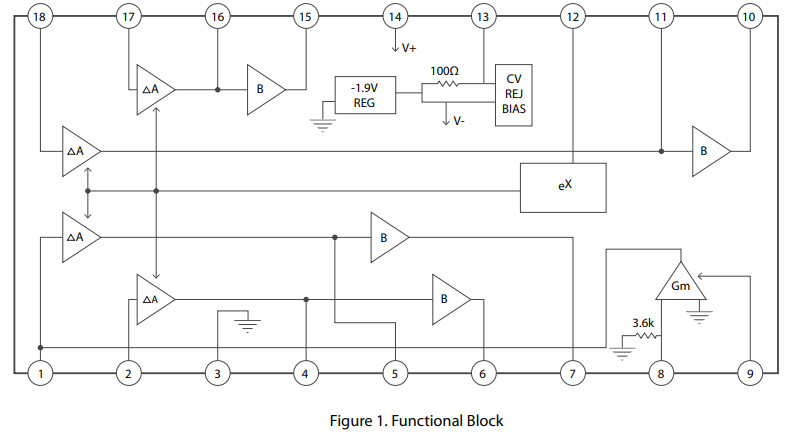
Functional Block Diagram
Absolute Maximum Ratings
| Description | Symbol | Value range | Unit |
| Voltage Between VCC and VEE | VVCC-VEE | –0.5~+22 | V |
| Voltage Between VCC and Ground | VVCC-GND | -0.5-+18 | V |
| Voltage Between VEE and Ground | VVEE GND | -4-+0.5 | V |
| Voltage Between Frequency Control and Ground | Wreq Cntl- GND | -6-+6 | V |
| Voltage Between Resonance Control and Ground | VRes Cntl-GND | —18-4-2 | V |
| Current Through Any Pin | I | -40-+40 | mA |
| Storage Temperature Range | TSTG | -55-+150 | °C |
| Operating Free-air Temperature Range | TA | -25-+75 | °C |
Note: Stresses greater than those listed under “Absolute Maximum Ratings” may cause permanent damage to the device.These are stress ratings only, and functional operation of the device at these or any other conditions beyond those indicated under “Recommended Operating Conditions” is not implied. Exposure to “Absolute Maximum Ratings” for extended periods may affect device reliability.Electrical Characteristics(VCC = 15 V, RF = 100 K. A current limiting resistor is connected between -15 V and VSS, TA = +20 °C. Actual circuit connection sees typical application circuit, unless otherwise noted)
| Parameter | Symbol | Test Condition | Min. | Typ. | Max. | Unit |
| Pole FrequencyControl Range | pfc | — | 3500:01:00 | 10000:01:00 | — | Hz |
| Positive SupplyVoltage Range | VCC | — | 9 | — | 18 | V |
| Negative SupplyVoltage Range | VSS | Current limitingresistor alwaysrequired | -4 | — | -18 | V |
| Positive SupplyCurrent | I’ve | — | 4. | 5 | 7. | mA |
| Sensitivity of PoleFrequency ControlRange Scale, Midrange | S-Fp | — | 58. | 60 | 63. | mv/decade |
| Tempco of PoleFrequency ControlRange Scale | TEMP-Fp | — | 3000 | 3300 | 3500 | ppm |
| Exponential Errorof Pole FrequencyControl Range Scale | ER, | -25mV<Vc<155mV | — | 4 | 12 | % |
| Gain of VariableGain Cell | Gain | Vc=OV | 0.7 | 0.9 | 1. | — |
| Max Gain of VariableGain Cell | Gain-MAX | — | 2. | 3 | 4. | — |
| Tempco of VariableGain Cell | TEMP-Ganca | Vc=OV | 500 | 1500 | ppm | |
| Output Impendence ofGain Cell | RO-GainCell | Vc=OV | 0.5 | 1 | 2 | MO |
| Pole FrequencyControl Feed-through | WEED-FP | — | — | 60 | 200 | mV |
| Pole FrequencyWarm-up Drift | Drift-„ | -25°C<TA<75°C | — | 0.5 | 2. | 96 |
| Gm of Resonancecontrol Element | Gm-Ris | lok=100uA | 0.8 | 1 | 1. | mmhos |
| Amount of ResonanceObtainable BeforeOscillation | Amount-Fes | — | 20 | 30 | — | dB |
| Resonance ControlFeed-through | VFEED-RES | 0<lat<100UA | — | 0.2 | 2. | V |
| Output SwingAt Clipping | Output Swing | — | 10 | 12 | 14 | V.P.P |
| Output Noise reMax Output | / V P P VN.. | Low Pass and 20 Khzcut-off frequency | -76 | -86 | — | dB |
| Rejection inBand-reject | REJ-BANDRoca | — | 73 | 83 | — | dB |
| Distortion inPass-band | THD-mssemo | Output Signal is 3 dB below clipping point and Distortion is predominantly second harmonic | __ | 0.1 | 0.3 | 96 |
| Distortion inBand-reject | THD-SAMDREIET | Output Signal is 6 dB below clipping point and Distortion is predominantly second harmonic | __ | 0.3 | 1 | % |
| Distortion of SineWave Oscillation | THD-98, | Sinewave is notclipped by first stage | __ | 0.5 | 2. | 96 |
| Internal ReferenceCurrent | IKF | — | 45 | 63 | 85 | uA |
| Input Bias Current ofFrequency ControlInput | 181M-FON | FCIN=OV | 0.2 | 0.5 | 2. | uA |
| Input Impedanceto ResonanceSignal Input | Rin-,” | lAciti=150uA | 3. | 4. | 5. | KO |
| Buffer Slew Rate | SlhuFFER | — | 2. | 3 | – | V/us |
| Buffer InputBias Current | WS-BUM* | IEE=8mA | ±8 | ±30 | ±100 | nA |
| Buffer Sink Capability | l-seoc | — | 0.4 | 0.5 | 0.63 | mA |
| Buffer OutputImpedance | Ro-ellirut | Vc=0V | 75 | 100 | 200 | 0 |
Functional Description
- SuppliesA shunt regulator is built-in to regulate the negative supply at -1.9 volts. The shunt regulator can reduce the warm-up drift of the pole frequencies, at the same time, any negative supply greater than -4 volts can be used with the current limiting resistor. The value of the current limiting resistor is given by the following expression:
 Any positive supply between 9 volts and 18 volts can be applied to pin 14, but this will affect the output swing.The maximum possible peak to peak output swing is given by:
 - Operation of Each Filter stageEach filter section contains a variable gain cell and a high impedance buffer. The variable gain cell is a current-in, the current-out device, the output current IOUT is calculated as follows:Where VT = KT/q, VC is the voltage applied to pin 12, and AIO is the current gain of the cell at VC = 0, the IREF is givenFor normal operation of any filter type, each stage is set up with a feedback resistor and a pole capacitor.The feedback resistor, RF, is connected between variable gain cell input and buffer output, and the pole capacitor, CP, is connected to the output of the variable gain cell. Figure2 shows this setup, the output of the buffer will always adjust itself so that a current equal to IREF flows into the input.The quiescent output voltage of each buffer, VODC, should be set to 0.46VCC for the lowest control voltage feed-through and maximum peak-to-peak output signal, so the RF in Figure2 can be calculated as follows:The output impedance of the variable gain cell has reflected in the input as an A.C. resistance (nominally 1M) in parral with the feedback resistor regardless of the control voltage value. The total equivalent feedback resistance, REQ, determines the pole frequency of each filter section.
- Pole Frequency ControlThe voltage applied to pin 12 controls the current gain of each filter section because the exponential scale needs to meet the standard 18 mV/octave(60 mV/decade), an input attenuator network may be required in most case.An increasing positive control voltage will cause a drop of the pole frequency. If you want to get a thousand-to-one control range, the voltage applied to pin 12 should be maintained between -25 mV and 155 mV.
- Resonance ControlThe traditional transconductance type of amplifier can control the amount of resonance. Pin 8 is a separate signal voltage input and pin 9 is a separate control current input with a modified linear scale. The current output of the amplifier is internally connected to the input of stage one. The input impedance of the amplifier is 3.6 K ±900 Ω, and the input refers to ground, so a coupling capacitor is needed to be connected to the filter output.Control of the transconductance is accomplished with current input. Since the control input is a low impedance summing node, which is a potential near ground, the control current may be derived by an input resistor, RRC, from the resonance control voltage, at the same time, this resistor should meet the requirement that the maximum available resonance control voltage produces the maximum desired control current.
- Stage BuffersFor any sections, each buffer can source up to 10 mA and sink a nominal 500 uA, when any D.C. load greater than ±200 us to ±300 uA, the performance of the filter will drop, especially the loads on each buffer differ by more than this amount, so the maximum recommended D.C. loads are 1 mA source, 250 uA sink, and a 150 uA load difference between buffers. The maximum recommended A.C. loads are ±250 uA.The D.C. level of the filter output has been set to 0.46VCC (6.9 volts for VCC = 15 V), the coupling capacitor will be needed at the filter output or the following input of the device.
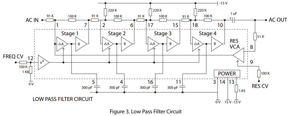
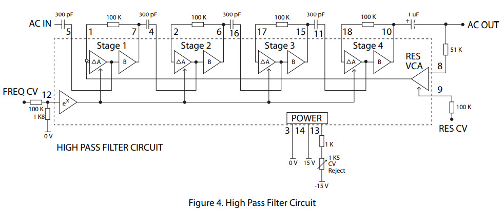
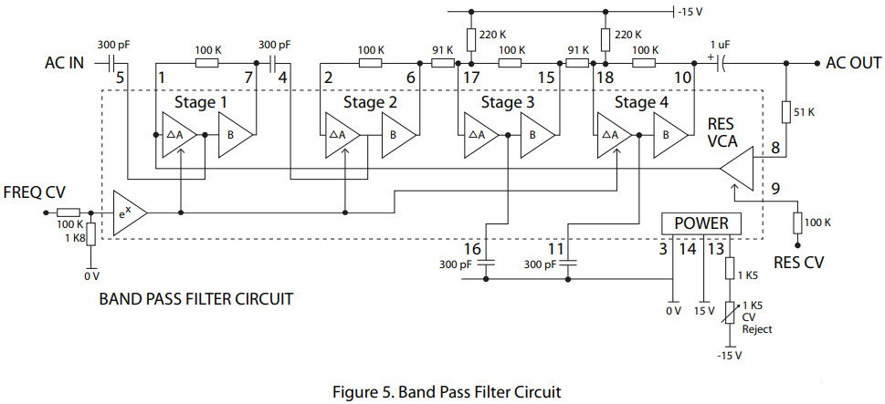
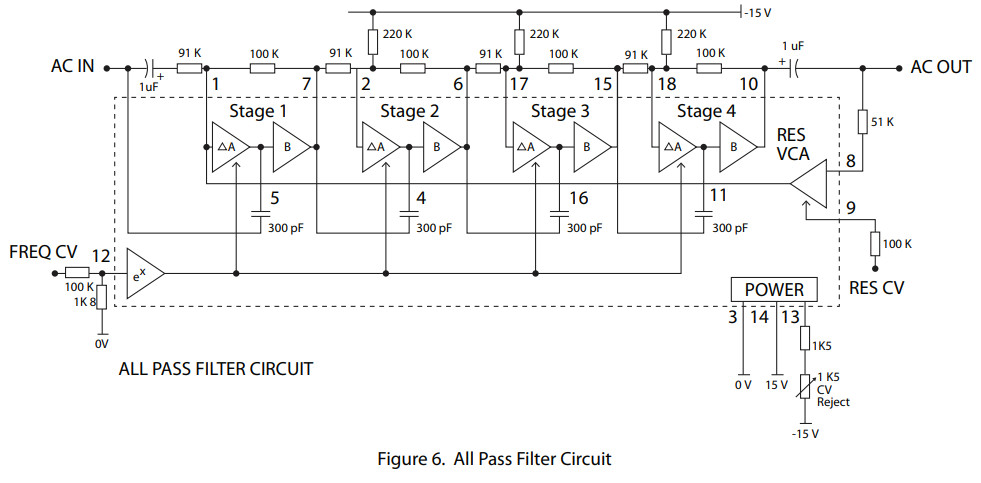
- Filter ResponsesIn the typical application circuit, Figures 3, 4, 5, and 6 show four filter responses: low pass, high pass, bandpass, and all pass. All filter responses have the function of voltage-controlled resonance, Since the configuration of the resonance feedback, the resonance frequency of the high pass will be about 2.4 times higher than low pass, however, the resonance frequency of the bandpass and all pass will be 0.42 times lower than the low pass.
 Any positive supply between 9 volts and 18 volts can be applied to pin 14, but this will affect the output swing.The maximum possible peak to peak output swing is given by:
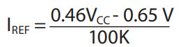 For normal operation of any filter type, each stage is set up with a feedback resistor and a pole capacitor.The feedback resistor, RF, is connected between variable gain cell input and buffer output, and the pole capacitor, CP, is connected to the output of the variable gain cell. Figure2 shows this setup, the output of the buffer will always adjust itself so that a current equal to IREF flows into the input.
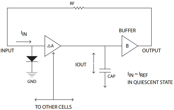 The quiescent output voltage of each buffer, VODC, should be set to 0.46VCC for the lowest control voltage feed-through and maximum peak-to-peak output signal, so the RF in Figure2 can be calculated as follows:
 The output impedance of the variable gain cell has reflected in the input as an A.C. resistance (nominally 1M) in parral with the feedback resistor regardless of the control voltage value. The total equivalent feedback resistance, REQ, determines the pole frequency of each filter section.
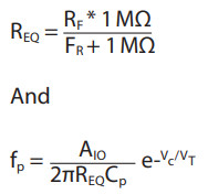
Typical Application Circuit
Package Information
SOP18L
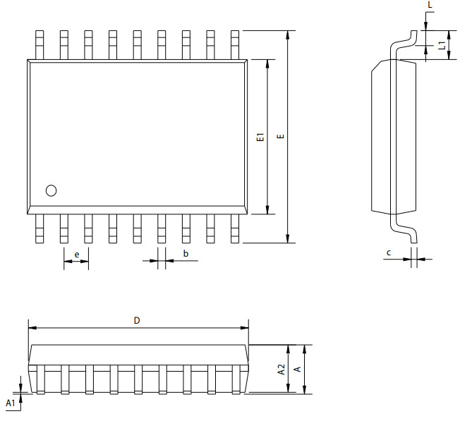
| SYMBOL | mm | |
| min | max | |
| A | — | 2.65 |
| Al | 0.10 | 0.30 |
| A2 | 2.20 | 2.40 |
| b | 0.35 | 0.45 |
| c | 0.20 | 0.30 |
| D | 11.25 | 12. |
| E | 10.10 | 10.50 |
| El | 7.30 | 7.70 |
| e | 1.27BSC | |
| L | 0.50 | 1.00 |
| Ll | 1.40BSC |
[xyz-ips snippet=”download-snippet”]