
![]()
FSR®Force Sensing Resistor®Integration Guide andEvaluation Parts Catalog
400 Series Evaluation PartsWith Suggested Electrical Interfaces
The product information contained in this document is designed to provide general information and guidelines only and must not be used as an implied contract with Interlink Electronics, Inc. Acknowledging our policy of continual product development, we reserve the right to change, without notice, and detail in this publication. Since Interlink Electronics has no control over the conditions and method of use of our products, we suggest that any potential user confirm their suitability before adopting them for commercial use.
FSR® Integration Guide & Evaluation Parts Catalog With Suggested Electrical Interfaces
Interlink Electronics manufactures custom FSR devices to meet the needs of specific customer applications. FSR devices can be produced in almost any shape, size, and geometry.
To discuss custom design or to obtain a quote, contact Interlink Electronics at (805) 484-8855.
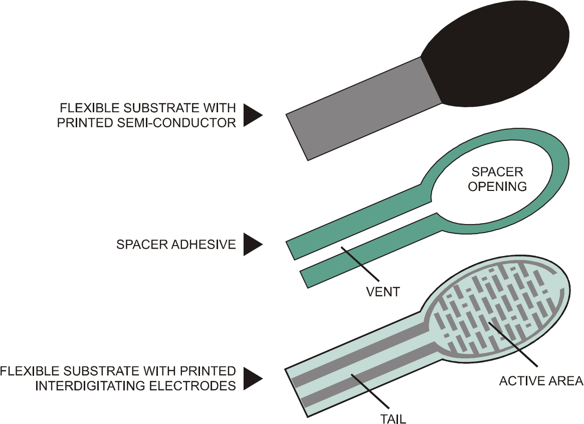
Figure 1: FSR Construction
Force Sensing Resistors®- An Overview of the Technology
Force Sensing Resistors (FSR) are a polymer thick film (PTF) device which exhibits a decrease in resistance with an increase in the force applied to the active surface. Its force sensitivity is optimized for use in human touch control of electronic devices. FSRs are not a load cell or strain gauge, though they have similar properties. FSRs are not suitable for precision measurements.
Force vs. Resistance
The force vs. resistance characteristic shown in Figure 2 provides an overview of FSR typical response behavior. For interpretational convenience, the force vs. resistance data is plotted on a log/log Figure 1: FSR Construction format. These data are representative of our typical devices, with this particular force-resistance characteristic being the response of evaluation part # 402 (0.5” [12.7 mm] diameter circular active area). A stainless steel actuator with a 0.4” [10.0 mm] diameter hemispherical tip of 60 durometer polyurethane rubber was used to actuate the FSR device. In general, FSR response approximately follows an inverse power-law characteristic (roughly 1/R). 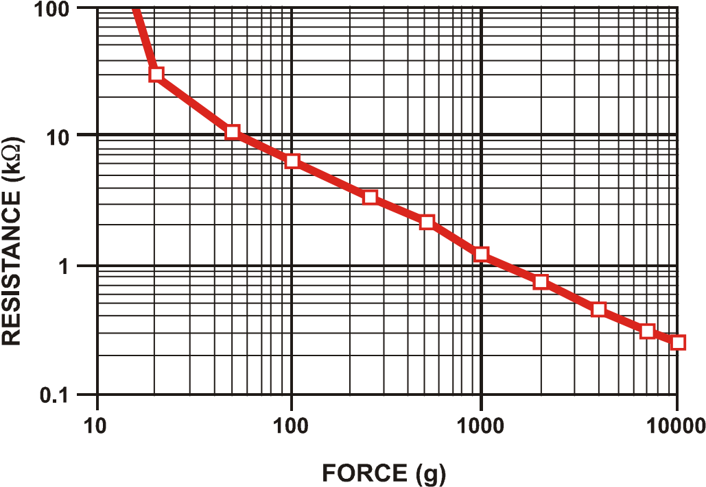
Figure 2: Resistance vs. Force
Referring to Figure 2, at the low force end of the force-resistance characteristic, a switchlike response is evident. This turn-on threshold, or ‘break force”, that swings the resistance from greater than 100 kΩ to about 10 kΩ (the beginning of the dynamic range that follows a power-law) is determined by the substrate and overlay thickness and flexibility, size and shape of the actuator, and spacer-adhesive thickness (the gap between the facing conductive elements). Break force increases with increasing substrate and overlay rigidity, actuator size, and spacer adhesive thickness. Eliminating the adhesive, or keeping it well away from the area where the force is being applied, such as the center of a large FSR device, will give it a lower rest resistance (e.g. stand-off resistance).
At the high force end of the dynamic range, the response deviates from the power-law behavior, and eventually saturates to a point where increases in force yield little or no decrease in resistance. Under these conditions of Figure 2, this saturation force is beyond 10 kg. The saturation point is more a function of pressure than force. The saturation pressure of a typical FSR is on the order of 100 to 200 psi. For the data shown in Figures 2, 3, and 4, the actually measured pressure range is 0 to 175 psi (0 to 22 lbs applied over 0.125 in2). Forces higher than the saturation force can be measured by spreading the force over a greater area; the overall pressure is then kept below the saturation point, and dynamic response is maintained. However, the converse of this effect is also true, smaller actuators will saturate FSRs earlier in the dynamic range since the saturation point is reached at a lower force. 
Figure 3:Conductance vs. Force (0-10Kg)
Force vs. Conductance
In Figure 3, the conductance is plotted vs. force (the inverse of resistance: 1/r). This format allows interpretation on a linear scale. For reference, the corresponding resistance values are also included on the right vertical axis. A simple circuit called a current-to-voltage converter (see page 21) gives a voltage output directly proportional to FSR conductance and can be useful where response linearity is desired. Figure 3 also includes a typical part-to-part repeatability envelope. This error band determines the maximum accuracy of any general force measurement. The spread or width of the band is strongly dependent on the repeatability of any actuating and measuring system, as well as the repeatability tolerance held by Interlink Electronics during FSR production. Typically, the part-to-part repeatability tolerance held during manufacturing ranges from ± 15% to ± 25% of an established nominal resistance.
Figure 4 highlights the 0-1 kg (0-2.2 lbs) range of the conductance-force characteristic. As in Figure 3, the corresponding resistance values are included for reference. This range is common to human interface applications. Since the conductance response in this range is fairly linear, the force resolution will be uniform and data interpretation simplified. The typical part-to-part error band is also shown for this touch range. In most human touch control applications this error is insignificant since human touch is fairly inaccurate. Human factors studies have shown that in this force range repeatability errors of less than ± 50% are difficult to discern by touch alone.

Figure 4:Conductance vs. Force (0-1Kg) Low Force Range
FSR Integration Notes A Step-by-Step Guide to Optimal Use
For best results, follow these seven steps when beginning any new product design, proof-of-concept, technology evaluation, or first prototype implementation:
- Start with Reasonable Expectations (Know Your Sensor)The FSR sensor is not a strain gauge, load cell or pressure transducer. While it can be used for dynamic measurement, only qualitative results are generally obtainable. Force accuracy ranges from approximately ± 5% to ± 25% depending on the consistency of the measurement and actuation system, the repeatability tolerance held in manufacturing, and the use of part calibration.Accuracy should not be confused with resolution. The force resolution of FSR devices is better than ± 0.5% of full use force.
- Choose the Sensor that Best Fits the Geometry of Your ApplicationUsually sensor size and shape are the limiting parameters in FSR integration, so any evaluation part should be chosen to fit the desired mechanical actuation system. In general, standard FSR products have a common semiconductor make-up and only by varying actuation methods (e.g. overlays and actuator areas) or electrical interfaces can different response characteristics be achieved.
- Set-up a Repeatable and Reproducible Mechanical Actuation SystemWhen designing the actuation mechanics, follow these guidelines to achieve the best force repeatability:• Provide a consistent force distribution. FSR response is very sensitive to the distribution of the applied force. In general, this precludes the use of dead weights for characterization since exact duplication of the weight distribution is rarely repeatable cycle-to-cycle. A consistent weight (force) distribution is more difficult to achieve than merely obtaining a consistent total applied weight (force). As long as the distribution is the same cycle-to-cycle, then repeatability will be maintained. The use of a thin elastomer between the applied force and the FSR can help absorb error from inconsistent force distributions.• Keep the actuator area, shape, and compliance constant. Charges in these parameters significantly alter the response characteristic of a given sensor. Any test, mock-up, or evaluation conditions should be closely matched to the final use conditions. The greater the cycle-to-cycle consistency of these parameters, the greater the device repeatability. In human interface applications where a finger is the mode of actuation, perfect control of these parameters is not generally possible. However, human force sensing is somewhat inaccurate; it is rarely sensitive enough to detect differences of less than ± 50%.• Control actuator placement. In cases where the actuator is to be smaller than the FSR active area, cycle-to-cycle consistency of actuator placement is necessary. (Caution: FSR layers are held together by an adhesive that surrounds the electrically active areas. If force is applied over an area which includes the adhesive, the resulting response characteristic will be drastically altered.) In an extreme case (e.g., a large, flat, hard actuator that bridges the bordering adhesive), the adhesive can present FSR actuation• Keep actuation cycle time consistent. Because of the time dependence of the FSR resistance to an applied force, it is important when characterizing the sensor system to assure that increasing loads (e.g. force ramps) are applied at consistent rates (cycle-to-cycle). Likewise, static force measurements must take into account FSR mechanical setting time. This time is dependent on the mechanics of actuation and the amount of force applied and is usually on the order of seconds.
- Use the Optimal Electronic InterfaceIn most product designs, the critical characteristic is Force vs. Output Voltage, which is controlled by the choice of interface electronics. A variety of interface solutions are detailed in the TechNote section of this guide. Summarized here are some suggested circuits for common FSR applications.• For FSR Pressure or Force Switches, use the simple interfaces detailed on pages 16 and 17.• For dynamic FSR measurements or Variable Controls, a current-to-voltage converter (see pages 18 and 19) is recommended. This circuit produces an output voltage that is inversely proportional to FSR resistance. Since the FSR resistance is roughly inversely proportional to applied force, the end result is a direct proportionality between force and voltage; in other words, this circuit gives roughly linear increases in output voltage for increases in applied force. This linearization of the response optimizes the resolution and simplifies data interpretation.
- Develop a Nominal Voltage Curve and Error Spread When a repeatable and reproducible system has been established, data from a group of FSR parts can be collected. Test several FSR parts in the system. Record the output voltage at various pre-selected force points throughout the range of interest. Once a family of curves is obtained, a nominal force vs. output voltage curve and the total force accuracy of the system can be determined.
- Use Part Calibration if Greater Accuracy is RequiredFor applications requiring the highest obtainable force accuracy, part calibration will be necessary. Two methods can be utilized: gain and offset trimming, and curve fitting.• Gain and offset trimming can be used as a simple method of calibration. The reference voltage and feedback resistor of the current-to-voltage converter are adjusted for each FSR to pull their responses closer to the nominal curve.• Curve fitting is the most complete calibration method. A parametric curve fit is done for the nominal curve of a set of FSR devices, and the resultant equation is stored for future use. Fit parameters are then established for each individual FSR (or sending element in an array) in the set. These parameters, along with the measured sensor resistance (or voltage), are inserted into the equation to obtain the force reading. If needed, temperature compensation can also be included in the equation.
- Refine the SystemSpurious results can normally be traced to sensor error or system error. If you have any questions, contact Interlink Electronics’ Sales Engineers to discuss your system and final data.
FSR Usage Tips The Do’s and Don’ts
- Do follow the seven steps of the FSR Integration Guide.
- Do, if possible, use a firm, flat and smooth mounting surface.
- Do be careful if applying FSR devices to curved surfaces. Pre-loading of the device can occur as the two opposed layers are forced into contact by the bending tension. The device will still function, but the dynamic range may be reduced and resistance drift could occur. The degree of curvature over which an FSR can be bent is a function of the size of the active area. The smaller the active area, the less effect a given curvature will have on the FSR’s response.
- Do avoid air bubbles and contamination when laminating the FSR to any surface. Use only thin, uniform adhesives, such as Scotch brand double-sided laminating adhesives. Cover the entire surface of the sensor.
- Do be careful of kinks or dents in active areas. They can cause false triggering of the sensors.
- Do protect the device from sharp objects. Use an overlay, such as a polycarbonate film or an elastomer, to prevent gouging of the FSR device.
- Do use soft rubber or a spring as part of the actuator in designs requiring some travel.
- Do not kink or crease the tail of the FSR device if you are bending it; this can cause breaks in the printed silver traces. The smallest suggested bend radius for the tails of evaluation parts is about 0.1” [2.5 mm]. In custom sensor designs, tails have been made that bend over radii of 0.03” (0.8 mm]. Also, be careful if bending the tail near the active area. This can cause stress on the active area and may result in pre-loading and false readings.
- Do not block the vent. FSR devices typically have an air vent that runs from the open active area down the length of the tail and out to the atmosphere. This vent assures pressure equilibrium with the environment, as well as allowing even loading and unloading of the device. Blocking this vent could cause FSRs to respond to any actuation in a non-repeatable manner. Also note, that if the device is to be used in a pressure chamber, the vented end will need to be kept vented to the outside of the chamber. This allows for the measurement of the differential pressure.
- Do not solder directly to the exposed silver traces. With flexible substrates, the solder joint will not hold and the substrate can easily melt and distort during the soldering. Use Interlink Electronics’ standard connection techniques, such as solderable tabs, housed female contacts, Z-axis conductive tapes, or ZIF (zero insertion force) style connectors.
- Do not use cyanoacrylate adhesives (e.g. Krazy Glue) and solder flux removing agents. These degrade the substrate and can lead to cracking.
- Do not apply excessive shear force. This can cause delamination of the layers.
- Do not exceed 1mA of current per square centimeter of applied force (actuator area). This can irreversibly damage the device.
Evaluation Parts Catalog Descriptions and Dimensions

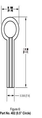
Figure 5:Part No. 400 (0.2” Circle)
Active Area: 0.2” [5.0] diameterNominal Thickness: 0.012” [0.30 mm]Material Build: Semiconductive layer0.004” [0.10] PES Spacer adhesive0.002” [0.05] AcrylicConductive layer 0.004” [0.10] PESRear adhesive0.002” [0.05] AcrylicConnector options
- No connector
- Solder Tabs (not shown)
- AMP Female connector Active Area: 0.5” [12.7] diameter
Nominal thickness: 0.018” [0.46 mm]Material Build:Semiconductive Layer 0.005” [0.13] UltemSpacer Adhesive0.006” [0.15] AcrylicConductive Layer 0.005” [0.13] UltemRear Adhesive0.002” [0.05] AcrylicConnector
- No connector
- Solder Tabs (not shown)
- AMP Female connector
Dimensions in brackets: millimeters • Dimensional Tolerance: ± 0.015” [0.4] • Thickness Tolerance: ± 10%
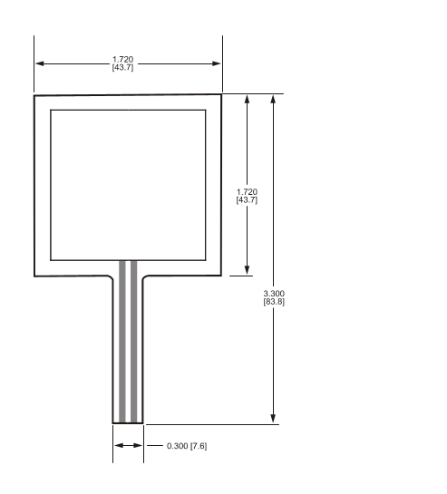
Figure 7: Part No. 406 (1.5” Square)
Active Area: 1.5” [38.1] x 1.5” [38.1]Nominal thickness: 0.018” [0.46 mm]
Material Build: Semiconductive Layer 0.005” [0.13] UltemSpacer Adhesive 0.006” [0.15] AcrylicConductive Layer 0.005” [0.13] UltemRear Adhesive 0.002” [0.05] AcrylicConnectors
- No connector
- Solder Tabs (not shown)
- AMP Female connector
Dimensions in brackets: millimeters • Dimensional Tolerance: ± 0.015” [0.4] • Thickness Tolerance: ± 10%
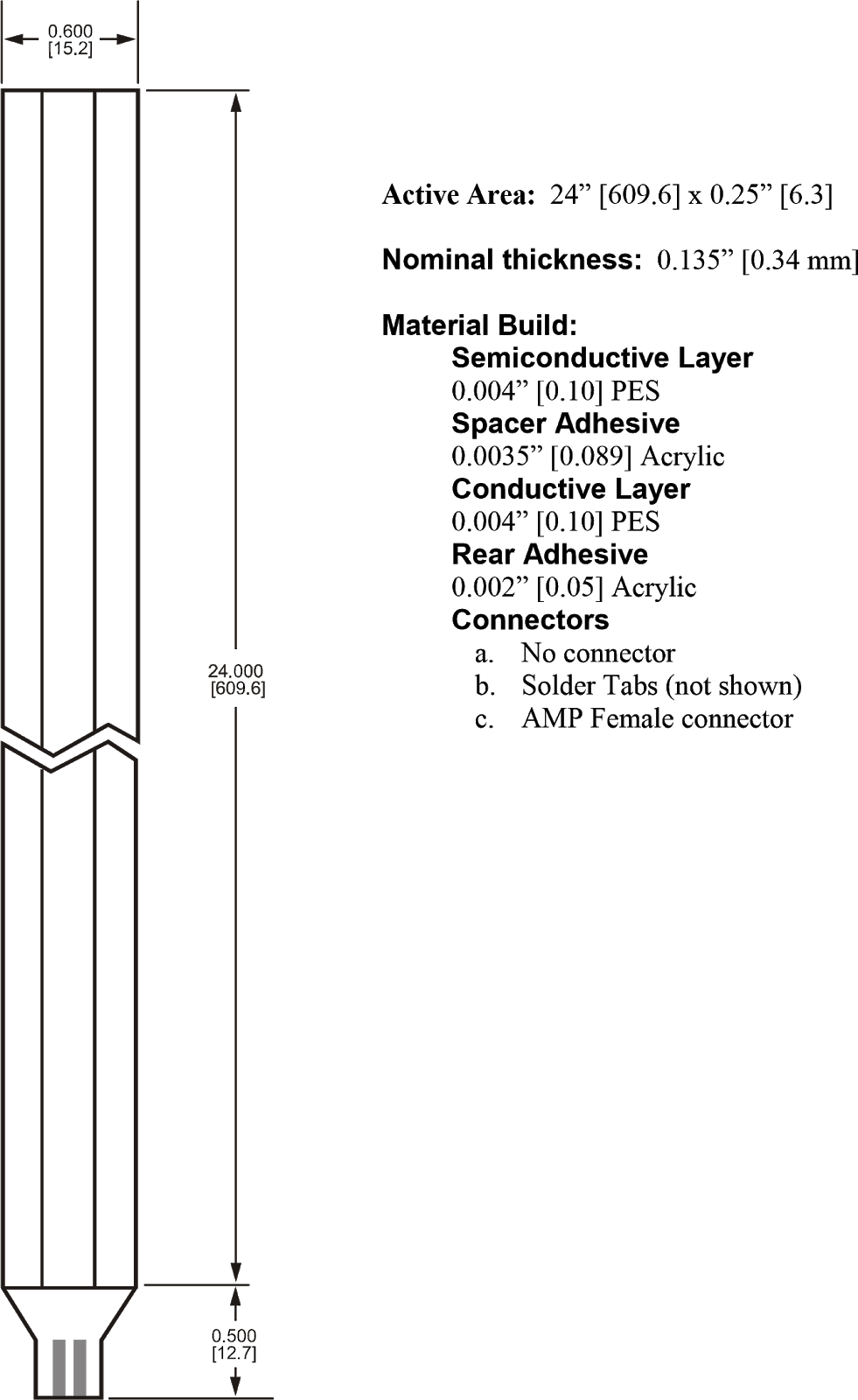
Figure 8Part No. 408 (24” Trimmable Strip)
Dimensions in brackets: millimetersDimensional Tolerance: ± 0.015” [0.4]Thickness Tolerance: ± 10%
General FSR Characteristics
These are typical parameters. The FSR is a custom device and can be made for use outside these characteristics. Consult Sales Engineering with your specific requirements.
Simple FSR Devices and Arrays
![]()
|
Size Range |
Max = 20” x 24” (51 x 61 cm) Min = 0.2” x 0.2” (0.5 x 0.5 cm) |
Any shape |
|
Device thickness |
0.008” to 0.050” (0.20 to 1.25 mm) |
Dependent on materials |
|
Force Sensitivity Range |
< 100 g to > 10 kg |
Dependent on mechanics |
|
Pressure Sensitivity Range |
< 1.5 psi to > 150 psi (< 0.1 kg/cm2 to > 10 kg/cm2) |
Dependent on mechanics |
|
Part-to-Part Force Repeatability |
± 15% to ± 25% of established nominal resistance |
With a repeatable actuation system |
|
Single Part Force Repeatability |
± 2% to ± 5% of established nominal resistance |
With a repeatable actuation system |
|
Force Resolution |
Better than 0.5% full scale |
|
|
Break Force (Turn-on Force) |
20 g to 100 g (0.7 oz to 3.5 oz) |
Dependent on mechanics and FSR build |
|
Stand-Off Resistance |
> 1MΩ |
Unloaded, unbent |
|
Switch Characteristic |
Essentially zero travel |
|
|
Device Rise Time |
1-2 msec (mechanical) |
|
|
Lifetime |
> 10 million actuations |
|
|
Temperature Range |
-30ºC to +70°C |
Dependent on materials |
|
Maximum Current |
I mA/cm2 of applied force |
|
|
Sensitivity to Noise/Vibration |
Not significantly affected |
|
|
EMI / ESD |
Passive device |
|
|
Lead Attachment |
Standard flex circuit techniques |
|
For Linear pots![]()
Positional Resolution 0.003” to 0.02” (0.075 to 0.5 mm) Dependent on actuator size
Positional Accuracy Better than ± 1% of full length
FSR terminology is defined on pages 14 and 15 of this guide.
The product information contained in this document is designed to provide general information and guidelines only and must not be used as an implied contract with Interlink Electronics. Acknowledging our policy of continual product development, we reserve the right to change without notice any detail in this publication. Since Interlink Electronics has no control over the conditions and method of use of our products, we suggest that any potential user confirm their suitability before adopting them for commercial use.
Glossary of Terms
Active AreaThe area of an FSR device that responds to normal force with a decrease in resistance.ActuatorThe object which contacts the sensor surface and applies force to FSRs.Applied ForceThe force applied by the actuator on the active area of the sensor.ArrayAny grouping or matrix of FSR sensors which can be individually actuated and measured.Break ForceThe minimum force required, with a specific actuator size, to cause the onset of the FSR response.Cross-talkMeasurement noise or inaccuracies of a sensor as a result of the actuation of another sensor on the same substrate. See also false triggering.DriffThe change in resistance with time under a constant (static) load. Also called resistance drift.DurometerThe measure of the hardness of rubber.EMIElectromagnetic interference.ESDElectrostatic discharge.False triggeringThe unwanted actuation of a FSR device from unexpected stimuli; e.g., bending or cross-talk.Fixed ResistorThe printed resistor on linear potentiometers that is used to measure position.FootprintSurface area and force distribution of the actuator in contact with the sensor surface.Force ResolutionThe smallest measurable difference in force.FSR™Force Sensing Resistors®. A polymer thick film device with exhibits a decrease in resistance with an increase in force applied normal to the device surface.Graphic OverlayA printed substrate that covers the FSR. Usually used for esthetics and protection.Housed FemaleA stitched on AMP connector with a receptacle (female) ending. A black plastic housing protects the contacts. Suitable for removable ribbon cable connector and header pin attachment.Hysteresis In a dynamic measurement, the difference between instantaneous force measurements at a given force for an increasing load versus a decreasing load.Interdigitating ElectrodesThe conductor grid. An interweaving pattern of linearly offset conductor traces used to achieve electrical contact. This grid is shunted by the semiconductor layer to give the FSR response.Lead Out or Busing SystemThe method of electrically accessing each individual sensor.Lexan®Polycarbonate. A substrate used for graphic overlays and labels. Available in a variety of surface textures.Melinex® A brand of polyester(PET). A substrate with lower temperature resistance than Ulterm® or PES, but with excellent flexibility and low cost. Similar to Mylar™.Part or DeviceThe FSR. Consists of the FSR semiconductive material, conductor, adhesives, graphics or overlays, and connectors.PES Polyethersulfone. A transparent substrate with excellent temperature resistance, moderate chemical resistance, and good flexibility.PinOutThe descriptions of a FSR’s electrical access at the connector pad (tail).Repeatability The ability to repeat, within a tolerance, a previous response characteristic.Response CharacteristicThe relationship of force or pressure vs. resistance.Saturation PressureThe pressure level beyond with the FSR response characteristic deviates from its inverse power law characteristic. Past the saturation pressure, increases in force yield little or no decrease in resistance.SensorEach area of the FSR device that is independently force sensitive (as in an array).Solder-tabs Stitched on AMP connectors with tab endings. Suitable for direct PC board connection or for soldering to wires.Space and TraceThe widths of the gaps and fingers of the conductive grid; also called pitch.Spacer AdhesiveThe adhesive used to laminate FSR devices tighter. Dictates stand-off.Stand-offThe gap or distance between the opposed polymer film layers when the sensor in unloaded and unbent.Stand-off ResistanceThe FSR resistance when the device is unloaded and unbent.SubstrateAny base material on which the FSR semi-conductive or metallic polymers are printed. (For example, polyetherimide, polyethersulfone and polyester films).TailThe region where the lead out or busing system terminates. Generally, the tail ends in a connector.Ulterm®Polyetherimide (PEI). A yellow, semi-transparent substrate with excellent temperature and chemical resistance and limited flexibility.
Interlink Electronics, Inc. holds international patents for its Force Sensign Resistor technology.
FSR is a trademark and Force Sensing Resistors is a registered trademark of Interlink Electronics. Interlink and the six dot logotype are registered marks or Interlink Electronics.
Ultem and Lexan are registered trademarks of G.E., Melinex is a registered trademark of ICI, and Mylar is a trademark of E.I. Dupont & Co.
Suggested Electrical Interfaces Basic FSRs

FSR Voltage Divider
For a simple force-to-voltage conversion, the FSR device is tied to a measuring resistor in a voltage divider configuration. The output is described by the equation:
VOUT = (V+) / [1 + RFSR/RM].
In the shown configuration, the output voltage increases with increasing force. If RFSR and RM are swapped, the output swing will decrease with increasing force. These two output forms are mirror images about the line VOUT = (V+) / 2.
The measuring resistor, RM, is chosen to maximize the desired force sensitivity range and to limit current. The current through the FSR should be limited to less than 1 mA/square cm of applied force. Suggested opamps for single-sided supply designs are LM358 and LM324. FET input devices such as LF355 and TL082 are also good. The low bias currents of these op-amps reduce the error due to the source impedance of the voltage divider.
A family of FORCE vs. VOUT curves is shown on the graph above for a standard FSR in a voltage divider configuration with various RM resistors. A (V+) of +5V was used for these examples.
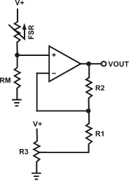 Figure 10Adjustable Buffer
Adjustable Buffers
Similar to the FSR Voltage Divider, these interfaces isolate the output from the high source impedance of the Force Sensing Resistor. However, these alternatives allow adjustment of the output offset and gain.
In Figure 10, the ratio of resistors R2 and R1 sets the gain of the output. Offsets resulting from the non-infinite FSR resistance at zero force (or bias currents) can be trimmed out with the potentiometer, R3. For best results, R3 should be about one-twentieth of R1 or R2. Adding an additional pot at R2 makes the gain easily adjustable. Broad range gain adjustment can be made by replacing R2 and R1 with a single pot.
The circuit in Figure 11 yields similar results to the previous one, but the offset trim is isolated from the adjustable gain. With this separation, there is no constraint on values for the pot. Typical cal for R5 and the pot are around 10kΩ.
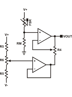 Figure 11Adjustable Buffer
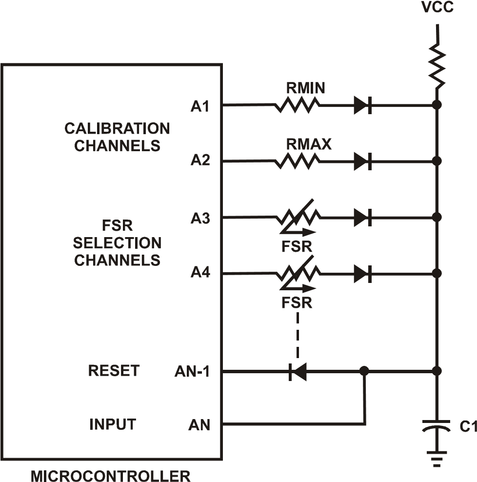
Figure 12Multi-Channel FSR-to-Digital Interface
Multi-Channel to FSR-to-Digital InterfaceSampling Cycle (any FSR channel):The microcontroller switches to a specific FSR channel, toggling it high, while all other FSR channels are toggled low. The RESET channel is toggled high, a counter starts, and the capacitor C1 charges, with its charging rate controlled by the resistance of the FSR (t ~ RC). When the capacitor reaches the high digital threshold of the INPUT channel, the counter shuts off, the RESET is toggled low, and the capacitor discharges.
The number of “counts” it takes from the toggling of the RESET high to the toggling of the INPUT high is proportional to the resistance of the FSR. The resistors RMIN and RMAX are used to set a minimum and maximum “counts” and therefore the range of the “counts”. They are also used periodically to re-calibrate the reference. A sampling cycle for RMIN is run, the number of “counts” is stored and used as a new zero. Similarly, a sampling cycle for RMAX is run and the value is stored as the maximum range (after subtracting the RMIN value). Successive FSR samplings are normalized to the new zero. The full range is “zoned” by dividing the normalized maximum “counts” by the number of desired zones. This will delineate the window size or width of each zone.
Continual sampling is done to record changes in FSR resistance due to change sin force. Each FSR is selected sequentially.
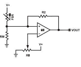 Figure 13FSR Variable Force Threshold Switch
FSR Variable Force Threshold Switch
This simple circuit is ideal for applications that require on-off switching at a specified force, such as touch-sensitive membrane, cut-off, and limit switches. For a variation of this circuit that is designed to control relay switching, see the following page.
The FSR device is arranged in a voltage divider with RM. An op-amp, U1, is used as a comparator. The output of U1 is either high or low. The non-inverting input of the op-amp is driven by the output of the divider, which is a voltage that increases with force. At zero force, the output of the op-amp will below. When the voltage at the non-inverting input of the op-amp exceeds the voltage of the inverting input, the output of the op-amp will toggle high. The triggering voltage, and therefore the force threshold, is set at the inverting input by the pot R1. The hysteresis, R2, acts as a “debouncer”, eliminating any multiple triggerings of the output that might occur.
Suggested op-amps are LM358 and LM324. Comparators like LM393 also work quite well. The parallel combination of R2 with RM is chosen to limit current and to maximize the desired force sensitivity range. A typical value for this combination is about 47kΩ.
The threshold adjustment pot, R1, can be replaced by two fixed value resistors in a voltage divider configuration.
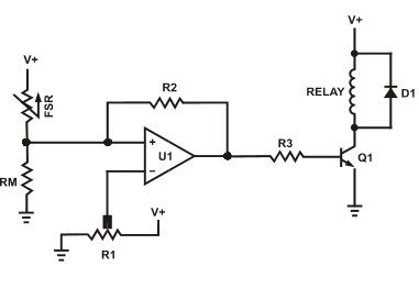 Figure 14FSR Variable Force Threshold Relay Switch
FSR Variable Force Threshold Relay Switch
This circuit is a derivative of the simple FSR Variable Force Threshold Switch on the previous page. It has use where the element to be switched requires higher current, like automotive and industrial control relays.
The FSR device is arranged in a voltage divider with RM. An op-amp, U1, is used as a comparator. The output of U1 is either high or low. The non-inverting input of the op-amp sees the output of the divider, which is a voltage that increases with force. At zero force, the output of the op-amp will below. When the voltage at the non-inverting input of the op-amp exceeds the voltage of the inverting input, the output of the op-amp will toggle high. The triggering voltage, and therefore the force threshold, is set at the inverting input by the pot R1. The transistor Q1 is chosen to match the required current specification for the relay.
Any medium power NPN transistor should suffice. For example, an NTE272 can sink 2 amps, and an NTE291 can sink 4 amps. The resistor R3 limits the base current (a suggested value is 4.7kΩ). The hysteresis resistor, R2, acts as a “debouncer’, eliminating any multiple triggerings of the output that might occur.
Suggested op-amps are LM358 and LM324. Comparators like LM393 and LM339 also work quite well, but must be used in conjunction with a pull-up resistor. The parallel combination of R2 with RM is chosen to limit current and to maximize the desired force sensitivity range. A typical value for this combination is about 47kΩ.
The threshold adjustment pot, R1, can be replaced by two fixed value resistors in a voltage divider configuration. The diode D1 is included to prevent flyback, which could harm the relay and the circuitry.
FSR Current-to-Voltage Converter
In this circuit, the FSR device is the input of a current-to-voltage converter. The output of this amplifier is described by the equation:
VOUT = VREF • [-RG/RFSR].
With a positive reference voltage, the output of the op-amp must be able to swing below ground, from 0V to –VREF, therefore dual-sided supplies are necessary. A negative reference voltage will yield a positive output swing, from 0V to +VREF.
VOUT = (-RG • VREF) /RFSR.
VOUT is inversely proportional to RFSR. Changing RG and/or VREF changes the response slope. The following is an example of the sequence used for choosing the component values and output swing:
For a human-to-machine variable control device, like a joystick, the maximum force applied to the FSR is about 1kg. Testing of a typical FSR shows that the corresponding RFSR at 1kg is about 4.6kΩ. If VREF is – 5V and an output swing of 0V to +5V is desired, then RG should be approximately equal to this minimum RFSR. RG is set at 4.7kΩ. A full swing of 0V to +5V is thus FSR Current-to-Voltage ConverterFigure 15 achieved. A set of FORCE vs. VOUT curves is shown in Figure 15 for a standard FSR using this interface with a variety of RG values.
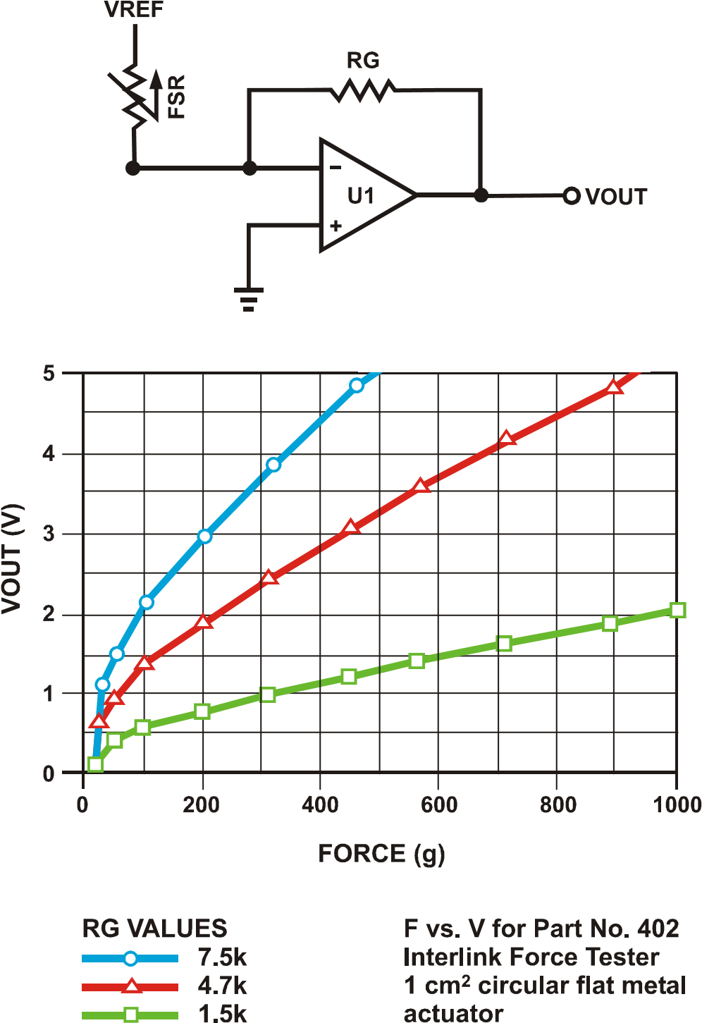
The current through the FSR device should be limited to less than 1 mA/square cm of applied force. As with the voltage divider circuit, adding a resistor in parallel with RFSR will give a definite rest voltage, which is essentially a zero-force intercept value. This can be useful when resolution at low forces is desired.

Figure 16Add’l FSR Current-to-Voltage Converter
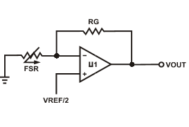
Figure 17Add’l FSR Current-to-Voltage Converter
Additional FSR Current-to-Voltage Converters
These circuits are a slightly modified version of the current-to-voltage converter detailed on the previous page. Please refer to it for more detail.
The output of Figure 16 is described by the equation:
VOUT = [VREF/2] * [1-RG/RFSR]
The output swing of this circuit is from (VREF/2) to 0V. In the case where RG is greater than RFSR, the output will go into negative saturation.
The output of Figure 17 is described by the equation:
VOUT = VREF/2 • [1 + RG/RFSR].
The output swing of this circuit is from (VREF/2) to VREF. In the case where RG is greater than RFSR, the output will go into positive saturation.
For either of these configurations, a zener diode placed in parallel with RG will limit the voltage built up across RG. These designs yield one-half the output swing of the previous circuit, but only require single-sided supplies and positive reference voltages. Like the preceding circuit, the current through the FSR should be limited to less than 1 mA/square cm of applied force.
Suggested op-amps are LM358 and LM324.

Figure 18FSR Schmitt Trigger Oscillator
FSR Schmitt Trigger Oscillator
In this circuit, an oscillator is made using the FSR device as the feedback element around a Schmitt Trigger. In this manner, a simple force-to-frequency converter is made. At zero force, the FSR is an open circuit. Depending on the last stage of the trigger, the output remains constant, either high or low. When the FSR is pressed, the oscillator starts, its frequency increasing with increasing force. The 2MΩ resistor at the input of the trigger ensures that the oscillator is off when FSRs with non-infinite resistance at zero force are used. The 47kΩ resistor and the 0.47 µF capacitor control the force-to-frequency characteristic. Changes in the “feel” of this circuit can be made by adjusting these values. The 0.1µF capacitor controls the frequency range of the oscillator. By implementing this circuit with CMOS or TTL, a digital process can be controlled by counting leading and/or trailing edges of the oscillator output. Suggested Schmitt Triggers are CD40106, CD4584, or 74C14.

546 Flynn Road • Camarillo, CA 93012805-484-8855 Phone • 805-484-8989 Fax
FSR Force Sensing Resistor Integration Guide and Evaluation Parts Catalog – FSR Force Sensing Resistor Integration Guide and Evaluation Parts Catalog –
[xyz-ips snippet=”download-snippet”]