life.augmented Value-line ARM Operation Datasheet STM32F030x4, STM32F030x6, STM32F030x8, STM32F030xC
Features
- Core: ARM® 32-bit Cortex®-M0 CPU, frequency up to 48 MHz
- Memories
- 16 to 256 Kbytes of Flash memory
- 4 to 32 Kbytes of SRAM with HW parity
- CRC calculation unit
- Reset and power management
- Digital & I/Os supply: VDD = 2.4 V to 3.6 V
- Analog supply: VDDA = VDD to 3.6 V
- Power-on/Power down reset (POR/PDR)
- Low power modes: Sleep, Stop, Standby
- Clock management
- 4 to 32 MHz crystal oscillator
- 32 kHz oscillator for RTC with calibration
- Internal 8 MHz RC with x6 PLL option
- Internal 40 kHz RC oscillator
- Up to 55 fast I/Os
- All mappable on external interrupt vectors
- Up to 55 I/Os with 5V tolerant capability
- 5-channel DMA controller
- One 12-bit, 1.0 μs ADC (up to 16 channels)
- Conversion range: 0 to 3.6 V
- Separate analog supply: 2.4 V to 3.6 V
- Calendar RTC with alarm and periodic wakeup from Stop/Standby
- 11 timers
- One 16-bit advanced-control timer for six-channel PWM output
- Up to seven 16-bit timers, with up to four IC/OC, OCN, usable for IR control decoding
- Independent and system watchdog timers
- SysTick timer
- Communication interfaces
- Up to two I2C interfaces
- one supporting Fast Mode Plus (1 Mbit/s) with 20 mA current sink,
- one supporting SMBus/PMBus.
- Up to six USARTs supporting master synchronous SPI and modem control; one with auto baud rate detection
- Up to two SPIs (18 Mbit/s) with 4 to 16 programmable bit frames
- Serial wire debug (SWD)
- All packages ECOPACK®2
|
Table 1. Device summary |
|
| Reference | Part number |
| STM32F030x4 | STM32F030F4 |
| STM32F030x6 | STM32F030C6, STM32F030K6 |
| STM32F030x8 | STM32F030C8, STM32F030R8 |
| STM32F030xC | STM32F030CC, STM32F030RC |
Introduction
This datasheet provides the ordering information and mechanical device characteristics of the STM32F030x4/6/8/C microcontrollers.This document should be read in conjunction with the STM32F0x0xx reference manual (RM0360). The reference manual is available from the STMicroelectronics website www.st.com.For information on the ARM® Cortex®-M0 core, please refer to the Cortex®-M0 Technical Reference Manual, available from the www.arm.com website.

Description
The STM32F030x4/6/8/C microcontrollers incorporate the high-performance ARM® Cortex®-M0 32-bit RISC core operating at a 48 MHz frequency, high-speed embedded memories (up to 256 Kbytes of Flash memory and up to 32 Kbytes of SRAM), and an extensive range of enhanced peripherals and I/Os. All devices offer standard communication interfaces (up to two I2Cs, up to two SPIs and up to six USARTs), one 12-bit ADC, seven general-purpose 16-bit timers and an advanced-control PWM timer.
The STM32F030x4/6/8/C microcontrollers operate in the -40 to +85 °C temperature range from a 2.4 to 3.6V power supply. A comprehensive set of power-saving modes allows the design of low-power applications.
The STM32F030x4/6/8/C microcontrollers include devices in four different packages ranging from 20 pins to 64 pins. Depending on the device chosen, different sets of peripherals are included. The description below provides an overview of the complete range of STM32F030x4/6/8/C peripherals proposed.
These features make the STM32F030x4/6/8/C microcontrollers suitable for a wide range of applications such as application control and user interfaces, handheld equipment, A/V receivers and digital TV, PC peripherals, gaming and GPS platforms, industrial applications, PLCs, inverters, printers, scanners, alarm systems, video intercoms, and HVACs.
Table 2. STM32F030x4/6/8/C family device features and peripheral counts
- TIM15 is not present.
- TIM7 is not present.
- SPI2 is not present.
- I2C2 is not present.
- USART2 to USART6 are not present.
- USART3 to USART6 are not present
Figure 1. Block diagram
- TIMER6, TIMER15, SPI, USART2 and I2C2 are available on STM32F030x8/C devices only.
- USART3, USART4, USART5 and USART6 are available on STM32F030xC devices only.
Functional overview
ARM®-Cortex®-M0 core with embedded Flash and SRAM
The ARM® Cortex®-M0 processor is the latest generation of ARM processors for embedded systems. It has been developed to provide a low-cost platform that meets the needs of MCU implementation, with a reduced pin count and low-power consumption, while delivering outstanding computational performance and an advanced system response to interrupts.The ARM® Cortex®-M0 32-bit RISC processor features exceptional code-efficiency, delivering the high-performance expected from an ARM core in the memory size usually associated with 8- and 16-bit devices.The STM32F0xx family has an embedded ARM core and is therefore compatible with all ARM tools and software.Figure 3 shows the general block diagram of the device family.
Memories
The device has the following features:
- • 4 to 32 Kbytes of embedded SRAM accessed (read/write) at CPU clock speed with 0wait states and featuring embedded parity checking with exception generation for failcritical applications.
- The non-volatile memory is divided into two arrays:
- 16 to 256 Kbytes of embedded Flash memory for programs and data
- Option bytes The option bytes are used to write-protect the memory (with 4 KB granularity) and/or readout-protect the whole memory with the following options:
- Level 0: no readout protection
- Level 1: memory readout protection, the Flash memory cannot be read from or written to if either debug features are connected or boot in RAM is selected
- Level 2: chip readout protection, debug features (Cortex®-M0 serial wire) and boot in RAM selection disabled
Boot modes
At startup, the boot pin and boot selector option bit are used to select one of the three boot options:
- Boot from User Flash
- Boot from System Memory
- Boot from embedded SRAM
The boot loader is located in System Memory. It is used to reprogram the Flash memory by using USART on pins PA14/PA15 or PA9/PA10
Cyclic redundancy check calculation unit (CRC)
The CRC (cyclic redundancy check) calculation unit is used to get a CRC code using a configurable generator polynomial value and size.Among other applications, CRC-based techniques are used to verify data transmission or storage integrity. In the scope of the EN/IEC 60335-1 standard, they offer a means of verifying the Flash memory integrity. The CRC calculation unit helps compute a signature of the software during runtime, to be compared with a reference signature generated at linktime and stored at a given memory location.
Power management
Power supply schemes
- VDD = 2.4 to 3.6 V: external power supply for I/Os and the internal regulator. Provided externally through VDD pins.
- VDDA = from VDD to 3.6 V: external analog power supply for ADC, Reset blocks, RCs and PLL (minimum voltage to be applied to VDDA is 2.4 V when the ADC is used). The VDDA voltage level must be always greater or equal to the VDD voltage level and must be provided first.For more details on how to connect power pins, refer to Figure 12: Power supply scheme
Power supply supervisorsThe device has integrated power-on reset (POR) and power-down reset (PDR) circuits. They are always active, and ensure proper operation above a threshold of 2 V. The device remains in reset mode when the monitored supply voltage is below a specified threshold, VPOR/PDR, without the need for an external reset circuit.
- The POR monitors only the VDD supply voltage. During the startup phase it is required that VDDA should arrive first and be greater than or equal to VDD.
- The PDR monitors both the VDD and VDDA supply voltages, however the VDDA power supply supervisor can be disabled (by programming a dedicated Option bit) to reduce the power consumption if the application design ensures that VDDA is higher than or equal to VDD.
Voltage regulatorThe regulator has two operating modes and it is always enabled after reset.
- Main (MR) is used in normal operating mode (Run).
- Low power (LPR) can be used in Stop mode where the power demand is reduced.
In Standby mode, it is put in power down mode. In this mode, the regulator output is in high impedance and the kernel circuitry is powered down, inducing zero consumption (but the contents of the registers and SRAM are lost).
Low-power modesThe STM32F030x4/6/8/C microcontrollers support three low-power modes to achieve the best compromise between low power consumption, short startup time and available wakeup sources:
- Sleep modeIn Sleep mode, only the CPU is stopped. All peripherals continue to operate and can wake up the CPU when an interrupt/event occurs.
- Stop modeStop mode achieves very low power consumption while retaining the content of SRAM and registers. All clocks in the 1.8 V domain are stopped, the PLL, the HSI RC and the HSE crystal oscillators are disabled. The voltage regulator can also be put either in normal or in low power mode.The device can be woken up from Stop mode by any of the EXTI lines. The EXTI line source can be one of the 16 external lines and RTC.
- Standby modeThe Standby mode is used to achieve the lowest power consumption. The internal voltage regulator is switched off so that the entire 1.8 V domain is powered off. The PLL, the HSI RC and the HSE crystal oscillators are also switched off. After entering Standby mode, SRAM and register contents are lost except for registers in the RTC domain and Standby circuitry.The device exits Standby mode when an external reset (NRST pin), an IWDG reset, a rising edge on the WKUP pins, or an RTC event occurs.
Note: The RTC, the IWDG, and the corresponding clock sources are not stopped by entering Stop or Standby mode.
Clocks and startup
System clock selection is performed on startup, however the internal RC 8 MHz oscillator is selected as default CPU clock on reset. An external 4-32 MHz clock can be selected, in which case it is monitored for failure. If failure is detected, the system automatically switches back to the internal RC oscillator. A software interrupt is generated if enabled. Similarly, full interrupt management of the PLL clock entry is available when necessary (for example on failure of an indirectly used external crystal, resonator or oscillator).Several prescalers allow the application to configure the frequency of the AHB and the APB domains. The maximum frequency of the AHB and the APB domains is 48 MHz.
Figure 2. Clock tree
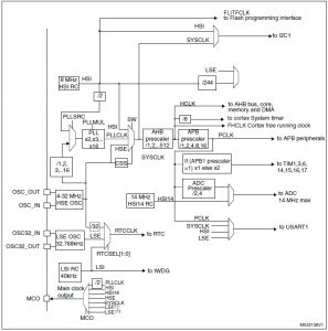
- LSI/LSE is not available in STM32F030x8 devices.
General-purpose inputs/outputs (GPIOs)
Each of the GPIO pins can be configured by software as output (push-pull or open-drain), as input (with or without pull-up or pull-down) or as peripheral alternate function. Most of the GPIO pins are shared with digital or analog alternate functions.
The I/O configuration can be locked if needed following a specific sequence in order to avoid spurious writing to the I/Os registers.
Direct memory access controller (DMA)
The 5-channel general-purpose DMA manages memory-to-memory, peripheral-to-memory and memory-to-peripheral transfers. The DMA supports circular buffer management, removing the need for user code intervention when the controller reaches the end of the buffer.
Each channel is connected to dedicated hardware DMA requests, with support for software trigger on each channel. Configuration is made by software and transfer sizes between source and destination are independent.
The DMA can be used with the main peripherals: SPI, I2C, USART, all TIMx timers (except TIM14) and ADC.
Interrupts and events
Nested vectored interrupt controller (NVIC)
The STM32F0xx family embeds a nested vectored interrupt controller able to handle up to 32 maskable interrupt channels (not including the 16 interrupt lines of Cortex®-M0) and 4 priority levels.
- Closely coupled NVIC gives low latency interrupt processing
- Interrupt entry vector table address passed directly to the core
- Closely coupled NVIC core interface
- Allows early processing of interrupts
- Processing of late arriving higher priority interrupts
- Support for tail-chaining
- Processor state automatically saved
- Interrupt entry restored on interrupt exit with no instruction overhead
This hardware block provides flexible interrupt management features with minimal interrupt latency.
Extended interrupt/event controller (EXTI)
The extended interrupt/event controller consists of 32 edge detector lines used to generate interrupt/event requests and wake-up the system. Each line can be independently configured to select the trigger event (rising edge, falling edge, both) and can be masked independently. A pending register maintains the status of the interrupt requests. The EXTI can detect an external line with a pulse width shorter than the internal clock period. Up to 55 GPIOs can be connected to the 16 external interrupt lines.
Analog to digital converter (ADC)
The 12-bit analog to digital converter has up to 16 external and two internal (temperature sensor, voltage reference measurement) channels and performs conversions in single-shot or scan modes. In scan mode, automatic conversion is performed on a selected group of analog inputs.The ADC can be served by the DMA controller.An analog watchdog feature allows very precise monitoring of the converted voltage of one, some or all selected channels. An interrupt is generated when the converted voltage is outside the programmed thresholds.
Temperature sensor
The temperature sensor (TS) generates a voltage VSENSE that varies linearly with temperature.The temperature sensor is internally connected to the ADC_IN16 input channel which is used to convert the sensor output voltage into a digital value. The sensor provides good linearity but it has to be calibrated to obtain good overall accuracy of the temperature measurement. As the offset of the temperature sensor variesfrom chip to chip due to process variation, the uncalibrated internal temperature sensor is suitable for applications that detect temperature changes only.To improve the accuracy of the temperature sensor measurement, each device isindividually factory-calibrated by ST. The temperature sensor factory calibration data are stored by ST in the system memory area, accessible in read-only mode.
Table 3. Temperature sensor calibration values
| Calibration value name | Description | Memory address |
| TS_CAL1 | TS ADC raw data acquired at a temperature of 30 °C (± 5 °C), VDDA= 3.3 V (± 10 mV) | 0x1FFF F7B8 – 0x1FFF F7B9 |
Internal voltage reference (VREFINT)
The internal voltage reference (VREFINT) provides a stable (bandgap) voltage output for the ADC. VREFINT is internally connected to the ADC_IN17 input channel. The precise voltage of VREFINT is individually measured for each part by ST during production test and stored in the system memory area. It is accessible in read-only mode.
Table 4. Internal voltage reference calibration values
| Calibration value name | Description | Memory address |
| VREFINT_CAL | Raw data acquired at a temperature of 30 °C (± 5 °C), VDDA= 3.3 V (± 10 mV) | 0x1FFF F7BA – 0x1FFF F7BB |
Timers and watchdogs
The STM32F030x4/6/8/C devices include up to six general-purpose timers, two basic timers and one advanced control timer.Table 5 compares the features of the different timers.
Table 5. Timer feature comparison
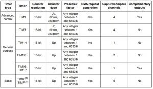
- Available on STM32F030x8 and STM32F030xB devices only.
- Available on STM32F030xB devices only
Advanced-control timer (TIM1)
The advanced-control timer (TIM1) can be seen as a three-phase PWM multiplexed on six channels. It has complementary PWM outputs with programmable inserted dead times. It can also be seen as a complete general-purpose timer. The four independent channels can be used for:
- Input capture
- Output compare
- PWM generation (edge or center-aligned modes)
- One-pulse mode output
If configured as a standard 16-bit timer, it has the same features as the TIMx timer. If configured as the 16-bit PWM generator, it has full modulation capability (0-100%).The counter can be frozen in debug mode.Many features are shared with those of the standard timers which have the samearchitecture. The advanced control timer can therefore work together with the other timers via the Timer Link feature for synchronization or event chaining.
General-purpose timers (TIM3, TIM14..17)
There are five synchronizable general-purpose timers embedded in theSTM32F030x4/6/8/C devices (see Table 5 for differences). Each general-purpose timer can be used to generate PWM outputs, or as simple time base
TIM3STM32F030x4/6/8/C devices feature one synchronizable 4-channel general-purpose timer. TIM3 is based on a 16-bit auto-reload up/downcounter and a 16-bit prescaler. It features four independent channels each for input capture/output compare, PWM or one-pulse mode output. This gives up to 12 input captures/output compares/PWMs on the largest packages.The TIM3 general-purpose timer can work with the TIM1 advanced-control timer via the Timer Link feature for synchronization or event chaining.TIM3 has an independent DMA request generation. This timer is capable of handling quadrature (incremental) encoder signals and the digitaloutputs from 1 to 3 hall-effect sensors. The counter can be frozen in debug mode.
TIM14This timer is based on a 16-bit auto-reload upcounter and a 16-bit prescaler.TIM14 features one single channel for input capture/output compare, PWM or one-pulse mode output. Its counter can be frozen in debug mode.
TIM15, TIM16 and TIM17These timers are based on a 16-bit auto-reload upcounter and a 16-bit prescaler.TIM15 has two independent channels, whereas TIM16 and TIM17 feature one single channel for input capture/output compare, PWM or one-pulse mode output.The TIM15, TIM16 and TIM17 timers can work together, and TIM15 can also operate withTIM1 via the Timer Link feature for synchronization or event chaining. TIM15 can be synchronized with TIM16 and TIM17.TIM15, TIM16 and TIM17 have a complementary output with dead-time generation and independent DMA request generation.Their counters can be frozen in debug mode.
Basic timers TIM6 and TIM7These timers can be used as a generic 16-bit time base.
Independent watchdog (IWDG)The independent watchdog is based on an 8-bit prescaler and 12-bit downcounter with user-defined refresh window. It is clocked from an independent 40 kHz internal RC and as it operates independently from the main clock, it can operate in Stop and Standby modes. It can be used either as a watchdog to reset the device when a problem occurs, or as a free running timer for application timeout management. It is hardware or software configurablethrough the option bytes. The counter can be frozen in debug mode.
System window watchdog (WWDG)The system window watchdog is based on a 7-bit downcounter that can be set as free running. It can be used as a watchdog to reset the device when a problem occurs. It is clocked from the APB clock (PCLK). It has an early warning interrupt capability and the counter can be frozen in debug mode.
SysTick timerThis timer is dedicated to real-time operating systems, but could also be used as a standard down counter. It features:
- A 24-bit down counter
- Autoreload capability
- Maskable system interrupt generation when the counter reaches 0
- Programmable clock source (HCLK or HCLK/8)
Real-time clock (RTC)
The RTC is an independent BCD timer/counter. Its main features are the following:
- Calendar with subseconds, seconds, minutes, hours (12 or 24 format), week day, date, month, year, in BCD (binary-coded decimal) format.
- Automatic correction for 28, 29 (leap year), 30, and 31 day of the month.
- Programmable alarm with wake up from Stop and Standby mode capability.
- Periodic wakeup unit with programmable resolution and period.
- On-the-fly correction from 1 to 32767 RTC clock pulses. This can be used to synchronize the RTC with a master clock.
- Digital calibration circuit with 1 ppm resolution, to compensate for quartz crystal inaccuracy.
- Tow anti-tamper detection pins with programmable filter. The MCU can be woken up from Stop and Standby modes on tamper event detection.
- Timestamp feature which can be used to save the calendar content. This function can be triggered by an event on the timestamp pin, or by a tamper event. The MCU can be woken up from Stop and Standby modes on timestamp event detection.
- Reference clock detection: a more precise second source clock (50 or 60 Hz) can be used to enhance the calendar precision.The RTC clock sources can be:
- A 32.768 kHz external crystal
- A resonator or oscillator
- The internal low-power RC oscillator (typical frequency of 40 kHz)
- The high-speed external clock divided by 32
Inter-integrated circuit interfaces (I2C)
Up to two I2C interfaces (I2C1 and I2C2) can operate in multimaster or slave modes. Both can support Standard mode (up to 100 kbit/s) or Fast mode (up to 400 kbit/s). I2C1 also supports Fast Mode Plus (up to 1 Mbit/s) with 20 mA output drive.Both support 7-bit and 10-bit addressing modes, multiple 7-bit slave addresses (two addresses, one with configurable mask). They also include programmable analog and digital noise filters.
Table 6. Comparison of I2C analog and digital filters
| Analog filter | Digital filter | |
| Pulse width of suppressed spikes | ≥ 50 ns | Programmable length from 1 to 15 I2C peripheral clocks |
| Benefits | Available in Stop mode | 1. Extra filtering capability vs. standard requirements.2. Stable length |
| Drawbacks | Variations depending on temperature, voltage, process |
In addition, I2C1 provides hardware support for SMBUS 2.0 and PMBUS 1.1: ARP capability, Host notify protocol, hardware CRC (PEC) generation/verification, timeouts verifications and ALERT protocol managementThe I2C interfaces can be served by the DMA controller. Refer to Table 7 for the differences between I2C1 and I2C2.
Table 7. STM32F030x4/6/8/C I2C implementation
| I2C features(1) | I2C1 | I2C2(2) |
| 7-bit addressing mode | X | X |
| 10-bit addressing mode | X | X |
| Standard mode (up to 100 kbit/s) | X | X |
| Fast mode (up to 400 kbit/s) | X | X |
| Fast Mode Plus (up to 1 Mbit/s) with 20mA output drive I/Os X -Independent clock | X | – |
| SMBus | X | – |
| Wakeup from STOP | – | – |
- X = supported.
- Only available on STM32F030x8/C devices.
Universal synchronous/asynchronous receiver transmitters(USART)
The device embeds up to six universal synchronous/asynchronous receiver transmitters (USART1, USART2 and USART3, USART4, USART5, USART6 on STM32F030xC devices only), which communicate at speeds of up to 6 Mbit/s.They provide hardware management of the CTS and RTS signals, multiprocessorcommunication mode, master synchronous communication and single-wire half-duplex communication mode. USART1 supports also the auto baud rate feature.The USART interfaces can be served by the DMA controller.
Table 8. STM32F030x4/6/8/C USART implementation(1)
| USART modes/features | USART1
|
USART2(2) | USART2(3),
USART3(3) |
USART4(3) | USART5(3)
|
USART6(3)
|
| Hardware flow control for modem | X | X | X | X | – | – |
| Continuous communication using DMA | X | X | X | X | X | X |
| Multiprocessor communication | X | X | X | X | X | X |
| Synchronous mode | X | X | X | X | X | – |
| Single-wire half-duplex communication | X | X | X | X | X | X |
| Receiver timeout interrupt | X | – | X | – | – | – |
| Auto baud rate detection | X | – | X | – | – | – |
- Where X means supported.
- Not available on STM32F030x4/6 devices.
- Available only on STM32F030xC devices.
Serial peripheral interface (SPI)
Up to two SPIs are able to communicate up to 18 Mbit/s in slave and master modes in fullduplex and half-duplex communication modes. The 3-bit prescaler gives 8 master mode frequencies and the frame size is configurable from 4 bits to 16 bits.SPI1 and SPI2 are identical and implement the set of features shown in the following table
Table 9. STM32F030x4/6/8/C SPI implementation
| SPI features(1) | SPI1 | SPI2(2) |
| Hardware CRC calculation | X | X |
| Rx/Tx FIFO | X | X |
| NSS pulse mode | X | X |
| TI mode | X | X |
- X = supported.
- Not available on STM32F030x4/6.
Serial wire debug port (SW-DP)
An ARM SW-DP interface is provided to allow a serial wire debugging tool to be connected to the MCU
Pinouts and pin descriptions
Figure 3. LQFP64 64-pin package pinout (top view), for STM32F030x4/6/8 devices
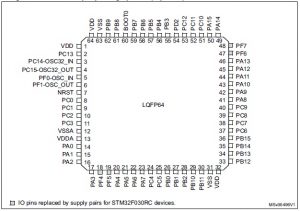
Figure 4. LQFP64 64-pin package pinout (top view), for STM32F030RC devices
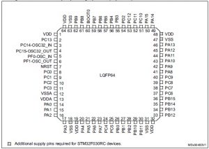
Figure 5. LQFP48 48-pin package pinout (top view), for STM32F030x4/6/8 devices
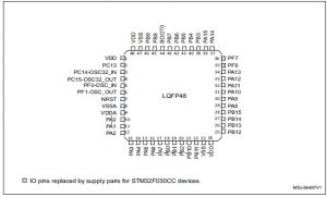
Figure 6. LQFP48 48-pin package pinout (top view), for STM32F030CC devices
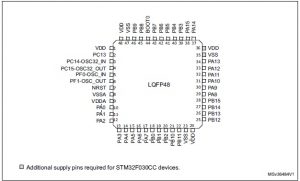
Figure 7. LQFP32 32-pin package pinout (top view)
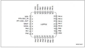
Figure 8. TSSOP20 20-pin package pinout (top view)
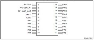
Table 10. Legend/abbreviations used in the pinout table
Table 11. STM32F030x4/6/8/C pin definitions
| Pin number | Pin name (function after reset) | Pin type | I/O structure | Notes | Pin functions | ||||
| LQFP64 | LQFP48 | LQFP32 | TSSOP20 | Alternate functions | Additional functions | ||||
| 1. | 1 | – | – | VDD | S | Complementary power supply | |||
| 2. | 2 | – | – | PC13 | I/O | TC | (1) | – | RTC_TAMP1, RTC_TS, RTC_OUT, WKUP2 |
| 3. | 3 | – | – | PC14-OSC32_IN (PC14) | I/O | TC | (1) | – | OSC32_IN |
| 4. | 4 | – | – | PC15-OSC32_OUT (PC15) | I/O | TC | (1) | – | OSC32_OUT |
| 5. | 5 | 2 | 2 | PF0-OSC_IN (PF0) | I/O | FT | I2C1_SDA(5) | OSC_IN | |
| 6. | 6 | 3 | 3 | PF1-OSC_OUT (PF1) | I/O | FT | I2C1_SCL(5) | OSC_OUT | |
| 7. | 7 | 4 | 4 | NRST | I/O | RST | Device reset input / internal reset output (active low) | ||
| 8. | — | – | – | PC0 | I/O | TTa | EVENTOUT, USART6_TX(5), USART7_TX(5) | ADC_IN10 | |
| 9. | – | – | – | PC1 | I/O | TTa | EVENTOUT, USART6_RX(5), USART7_RX(5) | ADC_IN11 | |
| 10. | – | – | – | PC2 | I/O | TTa | SPI2_MISO(5), EVENTOUT | ADC_IN12 | |
| 11. | – | – | – | PC3 | I/O | TTa | SPI2_MOSI(5), EVENTOUT | ADC_IN13 | |
| 12. | 8 | – | – | VSSA | S | Analog ground | |||
| 13. | 9 | 5 | 5 | VDDA | S | Analog power supply | |||
| 14. | 10 | 6 | 6 | PA0 | I/O | TTa | USART1_CTS(2), USART2_CTS(3)(5), USART4_TX(5) | ADC_IN0, RTC_TAMP2, WKUP1 | |
| 15. | 11 | 7 | 7 | PA1 | I/O | TTa | USART1_RTS(2), USART2_RTS(3)(5), EVENTOUT, USART4_RX(5) | ADC_IN1 | |
| 16. | 12 | 8 | 8 | PA2 | I/O | TTa | USART1_TX(2), USART2_TX(3)(5), TIM15_CH1(3)(5) | ADC_IN2 | |
| 17. | 13 | 9 | 9 | PA3 | I/O | TTa | USART1_RX(2), USART2_RX(3)(5), TIM15_CH2(3)(5) | ADC_IN3 | |
| 18. (4) | – | – | – | PF4 | I/O | TTa | (4) | EVENTOUT | – |
| 18(5) | – | – | – | VSS | I/O | TTa | (5) | Ground | |
| 19. (4) | – | – | – | PF5 | I/O | TTa | (4) | EVENTOUT | – |
| 19(5) | – | – | – | VDD | I/O | TTa | (5) | Complementary power supply | |
| 20. | 14 | 10 | 10 | PA4 | I/O | TTa | SPI1_NSS, USART1_CK(2) USART2_CK(3)(5), TIM14_CH1, USART6_TX(5) | ADC_IN4 | |
| 21. | 15 | 11 | 11 | PA5 | I/O | TTa | SPI1_SCK, USART6_RX(5) | ADC_IN5 | |
| 22. | 16 | 12 | 12 | PA6 | I/O | TTa | SPI1_MISO, TIM3_CH1, TIM1_BKIN, TIM16_CH1, EVENTOUT USART3_CTS(5) | ADC_IN6 | |
| 23. | 17 | 13 | 13 | PA7 | I/O | TTa | SPI1_MOSI, TIM3_CH2, TIM14_CH1, TIM1_CH1N, TIM17_CH1, EVENTOUT | ADC_IN7 | |
| 24. | – | – | – | PC4 | I/O | TTa | EVENTOUT, USART3_TX(5) | ADC_IN14 | |
| 25. | – | – | – | PC5 | I/O | TTa | USART3_RX(5) | ADC_IN15 | |
| 26. | 18 | 14 | – | PB0 | I/O | TTa | TIM3_CH3, TIM1_CH2N, EVENTOUT, USART3_CK(5) | ADC_IN8 | |
| 27. | 19 | 15 | 14 | PB1 | I/O | TTa | TIM3_CH4, TIM14_CH1, TIM1_CH3N, USART3_RTS(5) | ADC_IN9 | |
| 28. | 20 | – | – | PB2 | I/O | FT | (6) | – | – |
| 29. | 21 | – | – | PB10 | I/O | FT | SPI2_SCK(5), I2C1_SCL(2), I2C2_SCL(3)(5), USART3_TX(5) | – | |
| 30. | 22 | – | – | PB11 | I/O | FT | I2C1_SDA(2), I2C2_SDA(3)(5), EVENTOUT, USART3_RX(5) | – | |
| 31. | 23 | 16 | – | VSS | S | Ground | |||
| 32. | 24 | 17 | 16 | VDD | S | Digital power supply | |||
| 33. | 25 | – | – | PB12 | I/O | FT | SPI1_NSS(2), SPI2_NSS(3)(5), TIM1_BKIN, EVENTOUT, USART3_CK(5) | – | |
| 34. | 26 | – | – | PB13 | I/O | FT | SPI1_SCK(2), SPI2_SCK(3)(5), I2C2_SDA, TIM1_CH1N, USART3_CTS(5) | – | |
| 35. | 27 | – | – | PB14 | I/O | FT | SPI1_MISO(2), SPI2_MISO(3)(5), I2C2_SDA(5), TIM1_CH2N, TIM15_CH1(3)(5), USART3_RTS(5) | – | |
| 36. | 28 | – | – | PB15 | I/O | FT | SPI1_MOSI(2),
SPI2_MOSI(3)(5), TIM1_CH3N, TIM15_CH1N(3)(5), TIM15_CH2(3)(5) |
RTC_REFIN | |
| 37. | – | – | – | PC6 | I/O | FT | TIM3_CH1 | – | |
| 38. | – | – | – | PC7 | I/O | FT | TIM3_CH2 | – | |
| 39. | – | – | – | PC8 | I/O | FT | TIM3_CH3 | – | |
| 40. | – | – | – | PC9 | I/O | FT | TIM3_CH4 | – | |
| 41. | 29 | 18 | – | PA8 | I/O | FT | USART1_CK, TIM1_CH1, EVENTOUT, MCO | – | |
| 42. | 30 | 19 | 17 | PA9 | I/O | FT | USART1_TX, TIM1_CH2, TIM15_BKIN(3)(5) I2C1_SCL(2)(5) | – | |
| 43. | 31 | 20 | 18 | PA10 | I/O | FT | USART1_RX, TIM1_CH3, TIM17_BKIN I2C1_SDA(2)(5) | — | |
| 44. | 32 | 21 | – | PA11 | I/O | FT | USART1_CTS, TIM1_CH4, EVENTOUT, I2C2_SCL(5) | – | |
| 45. | 33 | 22 | – | PA12 | I/O | FT | USART1_RTS, TIM1_ETR, EVENTOUT, I2C2_SDA(5) | – | |
| 46. | 34 | 23 | 19 | PA13
(SWDIO) |
I/O | FT | (7) | IR_OUT, SWDIO | – |
| 47. (4)- | 35(4) | – | – | PF6 | I/O | FT | (4) | I2C1_SCL(2), I2C2_SCL(3) | – |
| 47 (5)- | 35(5) | – | – | VSS | I/O | FT | (5) | Ground- | |
| 48. (4) | 36(4) | – | – | PF7 | I/O | FT | (4) | I2C1_SDA(2), I2C2_SDA(3) | – |
| 48(5) | 36(5) | – | – | VDD | S | FT | (5) | Complementary power supply | |
| 49. | 37 | 24 | 20 | PA14
(SWCLK) |
I/O | FT | (7) | USART1_TX(2), USART2_TX(3)(5), SWCLK | – |
| 50. | 38 | 25 | – | PA15 | I/O | FT | SPI1_NSS, USART1_RX(2), USART2_RX(3)(5), USART4_RTS(5), EVENTOUT | – | |
| 51. | – | – | – | PC10 | I/O | FT | USART3_TX(5), USART4_TX(5) | – | |
| 52. | – | – | – | PC11 | I/O | FT | USART3_RX(5), USART4_RX(5) | – | |
| 53. | – | – | – | PC12 | I/O | FT | USART3_CK(5), USART4_CK(5), USART5_TX(5) | – | |
| 54. | – | – | – | PD2 | I/O | FT | TIM3_ETR, USART3_RTS(5), USART5_RX(5) | – | |
| 55. | 39 | 26 | – | PB2 | I/O | FT | SPI1_SCK, EVENTOUT, USART5_TX(5) | – | |
| 56. | 40 | 27 | – | PB4 | I/O | FT | SPI1_MISO, TIM3_CH1, EVENTOUT, TIM17_BKIN(5), USART5_RX(5) | ||
| 57. | 41 | 28 | – | PB5 | I/O | FT | SPI1_MOSI, I2C1_SMBA, TIM16_BKIN, TIM3_CH2, USART5_CK_RTS(5) | – | |
| 58. | 42 | 29 | – | PB6 | I/O | FTf | I2C1_SCL, USART1_TX, TIM16_CH1N | – | |
| 59. | 43 | 30 | – | PB7 | I/O | FTf | I2C1_SDA, USART1_RX, TIM17_CH1N, USART4_CTS(5) | – | |
| 60. | 44 | 31 | – | BOOT0 | I | B | Boot memory selection | ||
| 61. | 45 | – | – | PB8 | I/O | FTf | (7) | I2C1_SCL, TIM16_CH1 | – |
| 62. | 46 | – | – | PB9 | I/O | FTf | I2C1_SDA, IR_OUT, SPI2_NSS(5), TIM17_CH1, EVENTOUT | – | |
| 63. | 47 | 32 | 15 | VSS | S | Ground | |||
| 64. | 48 | 1 | 16 | VDD | S | Digital power supply |
- PC13, PC14 and PC15 are supplied through the power switch. Since the switch only sinks a limited amount of current (3 mA), the use of GPIOs PC13 to PC15 in output mode is limited:
- The speed should not exceed 2 MHz with a maximum load of 30 pF.
- These GPIOs must not be used as current sources (e.g. to drive an LED).
- This feature is available on STM32F030x6 and STM32F030x4 devices only.
- This feature is available on STM32F030x8 devices only.
- For STM32F030x4/6/8 devices only.
- For STM32F030xC devices only.
- On LQFP32 package, PB2 and PB8 should be treated as unconnected pins (even when they are not available on the package, they are not forced to a defined level by hardware).
- After reset, these pins are configured as SWDIO and SWCLK alternate functions, and the internal pull-up on SWDIO pin and internal pull-down on SWCLK pin are activated.
Table 12. Alternate functions selected through GPIOA_AFR registers for port A
- This feature is available on STM32F030x4 and STM32F030x6 devices only.
- This feature is available on STM32F030xC devices only
- This feature is available on STM32F030x8 devices only
Table 13. Alternate functions selected through GPIOB_AFR registers for port B
- This feature is available on STM32F030xC devices only
- This feature is available on STM32F030x4 and STM32F030x6 devices only.
- This feature is available on STM32F030x8 devices only.
Table 14. Alternate functions selected through GPIOC_AFR registers for port C
| Pin Name | AF0(1) | AF1(1) | AF2(1) |
| PC0 | EVENTOUT(1) | – | USART6_TX(1) |
| PC1 | EVENTOUT(1) | – | USART6_RX(1) |
| PC2 | EVENTOUT(1) | SPI2_MISO(1) | – |
| PC3 | EVENTOUT(1) | SPI2_MOSI(1) | – |
| PC4 | EVENTOUT(1) | USART3_TX(1) | – |
| PC5 | – | USART3_RX(1) | – |
| PC6 | TIM3_CH1(1) | – | – |
| PC7 | TIM3_CH2(1) | – | – |
| PC8 | TIM3_CH3(1) | – | – |
| PC9 | TIM3_CH4(1) | – | – |
| PC10 | USART4_TX(1) | USART3_TX(1) | – |
| PC11 | USART4_RX(1) | USART3_RX(1) | – |
| PC12 | USART4_CK(1) | USART3_CK(1) | USART5_TX(1) |
| PC13 | – | – | – |
| PC14 | – | – | – |
| PC15 | – | – | – |
- Available on STM32F030xC devices only
Table 15. Alternate functions selected through GPIOD_AFR registers for port D
| Pin Name | AF0(1) | AF1(1) | AF2 |
| PD2 | TIM3_ETR(1) | USART3_RTS(1) | USART5_RX(1) |
- Available on STM32F030xC devices only.
Table 16. Alternate functions selected through GPIOF_AFR registers for port F
| Pin Name | AF0 | AF1 |
| PF0 | – | I2C1_SDA(1) |
| PF1 | – | I2C1_SCL(1) |
- Available on STM32F030xC devices only.
Memory mapping
Figure 9. STM32F030x4/6/8/C memory map
Table 17. STM32F030x4/6/8/C peripheral register boundary addresses
| Bus | Boundary address | Size | Peripheral |
| 0x4800 1800 – 0x5FFF FFFF | ~384 MB | Reserved | |
| AHB2 | 0x4800 1400 – 0x4800 17FF | 1 KB | GPIOF |
| 0x4800 1000 – 0x4800 13FF | 1 KB | Reserved | |
| 0x4800 0C00 – 0x4800 0FFF | 1 KB | GPIOD | |
| 0x4800 0800 – 0x4800 0BFF | 1 KB | GPIOC | |
| 0x4800 0400 – 0x4800 07FF | 1 KB | GPIOB | |
| 0x4800 0000 – 0x4800 03FF | 1 KB | GPIOA | |
| 0x4002 4400 – 0x47FF FFFF | ~128 MB | Reserved | |
| AHB1 | 0x4002 3400 – 0x4002 43FF | 4 KB | Reserved |
| 0x4002 3000 – 0x4002 33FF | 1 KB | CRC | |
| 0x4002 2400 – 0x4002 2FFF | 3 KB | Reserved | |
| 0x4002 2000 – 0x4002 23FF | 1 KB FLASH | Interface | |
| 0x4002 1400 – 0x4002 1FFF | 3 KB | Reserved | |
| 0x4002 1000 – 0x4002 13FF | 1 KB | RCC | |
| 0x4002 0400 – 0x4002 0FFF | 3 KB | Reserved | |
| 0x4002 0000 – 0x4002 03FF | 1 KB | DMA | |
| APB | 0x4001 8000 – 0x4001 FFFF | 32 KB | Reserved |
| 0x4001 5C00 – 0x4001 7FFF | 9 KB | Reserved | |
| 0x4001 5800 – 0x4001 5BFF | 1 KB | DBGMCU | |
| 0x4001 4C00 – 0x4001 57FF | 3 KB | Reserved | |
| 0x4001 4800 – 0x4001 4BFF | 1 KB | TIM17 | |
| 0x4001 4400 – 0x4001 47FF | 1 KB | TIM16 | |
| 0x4001 4000 – 0x4001 43FF | 1 KB T | IM15(1) | |
| 0x4001 3C00 – 0x4001 3FFF | 1 KB | Reserved | |
| 0x4001 3800 – 0x4001 3BFF | 1 KB | USART1 | |
| 0x4001 3400 – 0x4001 37FF | 1 KB | Reserved | |
| 0x4001 3000 – 0x4001 33FF | 1 KB | SPI1 | |
| 0x4001 2C00 – 0x4001 2FFF | 1 KB | TIM1 | |
| 0x4001 2800 – 0x4001 2BFF | 1 KB | Reserved | |
| 0x4001 2400 – 0x4001 27FF | 1 KB | ADC | |
| 0x4001 1800 – 0x4001 23FF | 3 KB | Reserved | |
| 0x4001 1400 – 0x4001 17FF | 1 KB | USART6(2) | |
| 0x4001 0800 – 0x4001 13FF | 3 KB | Reserved | |
| 0x4001 0400 – 0x4001 07FF | 1 KB | EXTI | |
| 0x4001 0000 – 0x4001 03FF | 1 KB | SYSCFG | |
| 0x4000 8000 – 0x4000 FFFF | 32 KB | Reserved | |
| APB | 0x4000 7400 – 0x4000 7FFF | 3 KB | Reserved |
| 0x4000 7000 – 0x4000 73FF | 1 KB | PWR | |
| 0x4000 5C00 – 0x4000 6FFF | 5 KB | Reserved | |
| 0x4000 5800 – 0x4000 5BFF | 1 KB | I2C2(1) | |
| 0x4000 5400 – 0x4000 57FF | 1 KB | I2C1 | |
| 0x4000 5000 – 0x4000 53FF | 1 KB | USART5(2) | |
| 0x4000 4C00 – 0x4000 4FFF | 1 KB | USART4(2) | |
| 0x4000 4800 – 0x4000 4BFF | 1 KB | USART3(2) | |
| 0x4000 4400 – 0x4000 47FF | 1 KB | USART2(1) | |
| 0x4000 3C00 – 0x4000 43FF | 2 KB | Reserved | |
| 0x4000 3800 – 0x4000 3BFF | 1 KB | SPI2(1) | |
| 0x4000 3400 – 0x4000 37FF | 1 KB | Reserved | |
| 0x4000 3000 – 0x4000 33FF | 1 KB | IWDG | |
| 0x4000 2C00 – 0x4000 2FFF | 1 KB | WWDG | |
| 0x4000 2800 – 0x4000 2BFF | 1 KB | RTC | |
| 0x4000 2400 – 0x4000 27FF | 1 KB | Reserved | |
| 0x4000 2000 – 0x4000 23FF | 1 KB | TIM14 | |
| 0x4000 1800 – 0x4000 1FFF | 2 KB | Reserved | |
| 0x4000 1400 – 0x4000 17FF | 1 KB | TIM7(2) | |
| 0x4000 1000 – 0x4000 13FF | 1 KB | TIM6(1) | |
| 0x4000 0800 – 0x4000 0FFF | 2 KB | Reserved | |
| 0x4000 0400 – 0x4000 07FF | 1 KB | TIM3 | |
| 0x4000 0000 – 0x4000 03FF | 1 KB | Reserved |
- This feature is available on STM32F030x8 and STM32F030xC devices only. For STM32F030x6 and STM32F060x4, the area is Reserved.
- This feature is available on STM32F030xC devices only. This area is reserved for STM32F030x4/6/8 devices.
Electrical characteristics
Parameter conditions
Unless otherwise specified, all voltages are referenced to VSS
Minimum and maximum valuesUnless otherwise specified, the minimum and maximum values are guaranteed in the worst conditions of ambient temperature, supply voltage and frequencies by tests in production on 100% of the devices with an ambient temperature at TA = 25 °C and TA = TAmax (given by the selected temperature range).Data based on characterization results, design simulation and/or technology characteristics are indicated in the table footnotes and are not tested in production. Based on characterization, the minimum and maximum values refer to sample tests and represent the mean value plus or minus three times the standard deviation (mean ±3σ).
Typical valuesUnless otherwise specified, typical data are based on TA = 25 °C, VDD = VDDA = 3.3 V. They are given only as design guidelines and are not tested.Typical ADC accuracy values are determined by characterization of a batch of samples from a standard diffusion lot over the full temperature range, where 95% of the devices have anerror less than or equal to the value indicated (mean ±2σ).
Typical curvesUnless otherwise specified, all typical curves are given only as design guidelines and are not tested.
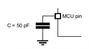
Loading capacitorThe loading conditions used for pin parameter measurement are shown in Figure 10.
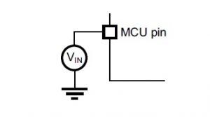
Pin input voltageThe input voltage measurement on a pin of the device is described in Figure 11.
| Figure 10. Pin loading conditions | Figure 11. Pin input voltage |
 |
|
Power supply scheme
Figure 12. Power supply scheme
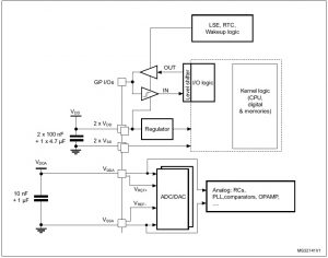
Caution: Each power supply pair (VDD/VSS, VDDA/VSSA etc.) must be decoupled with filtering ceramic capacitors as shown above. These capacitors must be placed as close as possible to, or below, the appropriate pins on the underside of the PCB to ensure the good functionality of the device.
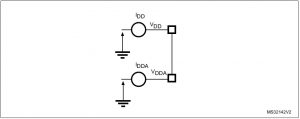
Current consumption measurement
Figure 13. Current consumption measurement scheme
Absolute maximum ratings
Stresses above the absolute maximum ratings listed in Table 18: Voltage characteristics, Table 19: Current characteristics and Table 20: Thermal characteristics may cause permanent damage to the device. These are stress ratings only and functional operation of the device at these conditions is not implied. Exposure to maximum rating conditions for extended periods may affect device reliability.
Table 18. Voltage characteristics(1)
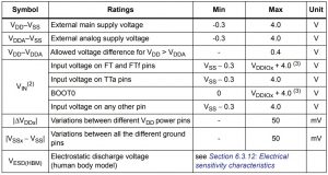
- All main power (VDD, VDDA) and ground (VSS, VSSA) pins must always be connected to the external power supply, in the permitted range.
- VIN maximum must always be respected. Refer to Table 19: Current characteristics for the maximum allowed injected current values.
- VDDIOx is internally connected with VDD pin.
Table 19. Current characteristics
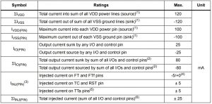
- All main power (VDD, VDDA) and ground (VSS, VSSA) pins must always be connected to the external power supply, in the permitted range.
- This current consumption must be correctly distributed over all I/Os and control pins. The total output current must not be sunk/sourced between two consecutive power supply pins referring to high pin count QFP packages.
- A positive injection is induced by VIN > VDDIOx while a negative injection is induced by VIN < VSS. IINJ(PIN) must never be exceeded. Refer to Table 18: Voltage characteristics for the maximum allowed input voltage values.
- Positive injection is not possible on these I/Os and does not occur for input voltages lower than the specified maximum value.
- On these I/Os, a positive injection is induced by VIN > VDDA. Negative injection disturbs the analog performance of the device. See note (2) below Table 52: ADC accuracy.
- When several inputs are submitted to a current injection, the maximum ΣIINJ(PIN) is the absolute sum of the positive and negative injected currents (instantaneous values).
Table 20. Thermal characteristics
| Symbol | Ratings | Value | Unit |
| TSTG | Storage temperature range | –65 to +150 | °C |
| TJ | Maximum junction temperature | 150 | °C |
Operating conditions
General operating conditions
Table 21. General operating conditions
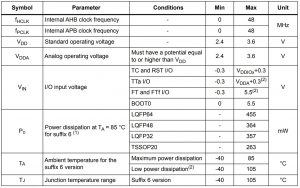
- If TA is lower, higher PD values are allowed as long as TJ does not exceed TJmax.
- In low power dissipation state, TA can be extended to this range as long as TJ does not exceed TJmax (see Section 7.2: Thermal characteristics).
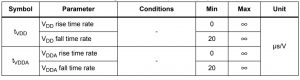
Operating conditions at power-up / power-down
The parameters given in Table 22 are derived from tests performed under the ambient temperature condition summarized in Table 21.
Table 22. Operating conditions at power-up / power-down
Embedded reset and power control block characteristics
The parameters given in Table 23 are derived from tests performed under the ambient temperature and supply voltage conditions summarized in Table 21: General operating conditions.
Table 23. Embedded reset and power control block characteristics
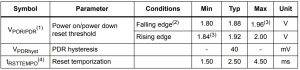
- The PDR detector monitors VDD and also VDDA (if kept enabled in the option bytes). The POR detector monitors only VDD.
- The product behavior is guaranteed by design down to the minimum VPOR/PDR value.
- Data based on characterization results, not tested in production.
- Guaranteed by design, not tested in production.
Embedded reference voltage
The parameters given in Table 24 are derived from tests performed under the ambient temperature and supply voltage conditions summarized in Table 21: General operating conditions
Table 24. Embedded internal reference voltage
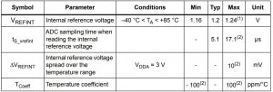
- Data based on characterization results, not tested in production.
- Guaranteed by design, not tested in production.
Supply current characteristicsThe current consumption is a function of several parameters and factors such as the operating voltage, ambient temperature, I/O pin loading, device software configuration, operating frequencies, I/O pin switching rate, program location in memory and executed binary code.
The current consumption is measured as described in Figure 13: Current consumption measurement scheme
All Run-mode current consumption measurements given in this section are performed with a reduced code that gives a consumption equivalent to CoreMark code.Typical and maximum current consumption The MCU is placed under the following conditions:
- All I/O pins are in analog input mode
- All peripherals are disabled except when explicitly mentioned
- The Flash memory access time is adjusted to the fHCLK frequency:
- 0 wait state and Prefetch OFF from 0 to 24 MHz
- 1 wait state and Prefetch ON above 24 MHz
- When the peripherals are enabled fPCLK = fHCLK
The parameters given in Table 25 to Table 27 are derived from tests performed under ambient temperature and supply voltage conditions summarized in Table 21: General operating conditions
Table 25. Typical and maximum current consumption from VDD supply at VDD = 3.6 V(1)
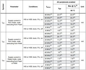
- The gray shading is used to distinguish the values for STM32F030xC devices.
- Data based on characterization results, not tested in production unless otherwise specified.
- For STM32F030x4/6/8 devices.
- For STM32F030xC devices only.
Table 26. Typical and maximum current consumption from the VDDA supply(1)
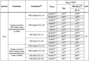
- The gray shading is used to distinguish the values for STM32F030xC devices.
- Current consumption from the VDDA supply is independent of whether the digital peripherals are enabled or disabled, being in Run or Sleep mode or executing from Flash or RAM. Furthermore, when the PLL is off, IDDA is independent from the frequency.
- Data based on characterization results, not tested in production.
- For STM32F030x4/6/8 devices.
- For STM32F030xC devices.
Table 27. Typical and maximum consumption in Stop and Standby modes
- Data based on characterization results, not tested in production unless otherwise specified.
Typical current consumptionThe MCU is placed under the following conditions:
- VDD = VDDA = 3.3 V
- All I/O pins are in analog input configuration
- The Flash access time is adjusted to fHCLK frequency:
- 0 wait state and Prefetch OFF from 0 to 24 MHz
- 1 wait state and Prefetch ON above 24 MHz
- When the peripherals are enabled, fPCLK = fHCLK
- PLL is used for frequencies greater than 8 MHz
- AHB prescaler of 2, 4, 8 and 16 is used for the frequencies 4 MHz, 2 MHz, 1 MHz and 500 kHz respectively
Table 28. Typical current consumption in Run mode, code with data processing running from Flash
I/O system current consumptionThe current consumption of the I/O system has two components: static and dynamic.
I/O static current consumptionAll the I/Os used as inputs with pull-up generate current consumption when the pin is externally held low. The value of this current consumption can be simply computed by using the pull-up/pull-down resistors values given in Table 46: I/O static characteristics. For the output pins, any external pull-down or external load must also be considered to estimate the current consumption.Additional I/O current consumption is due to I/Os configured as inputs if an intermediate voltage level is externally applied. This current consumption is caused by the input Schmitt trigger circuits used to discriminate the input value. Unless this specific configuration is required by the application, this supply current consumption can be avoided by configuring these I/Os in analog mode. This is notably the case of ADC input pins which should be configured as analog inputs.Caution: Any floating input pin can also settle to an intermediate voltage level or switch inadvertently, as a result of external electromagnetic noise. To avoid current consumption related to floating pins, they must either be configured in analog mode, or forced internally to a definite digital value. This can be done either by using pull-up/down resistors or by configuring the pins in output mode.I/O dynamic current consumption In addition to the internal peripheral current consumption measured previously, the I/Os used by an application also contribute to the current consumption. When an I/O pin switches, it uses the current from the I/O supply voltage to supply the I/O pin circuitry and tocharge/discharge the capacitive load (internal or external) connected to the pin:
ISW = VDDIO × f SW × C
where
ISW is the current sunk by a switching I/O to charge/discharge the capacitive load
VDDIOx is the I/O supply voltage
fSW is the I/O switching frequency
C is the total capacitance seen by the I/O pin: C = CINT + CEXT + CS
CS is the PCB board capacitance including the pad pin.
The test pin is configured in push-pull output mode and is toggled by software at a fixed frequency.
Table 29. Switching output I/O current consumption
- CS = 7 pF (estimated value).
Wakeup time from low-power modeThe wakeup times given in Table 30 are the latency between the event and the execution of the first user instruction. The device goes in low-power mode after the WFE (Wait For Event) instruction, in the case of a WFI (Wait For Interruption) instruction, 16 CPU cycles must be added to the following timings due to the interrupt latency in the Cortex M0 architecture.The SYSCLK clock source setting is kept unchanged after wakeup from Sleep mode. During wakeup from Stop or Standby mode, SYSCLK takes the default setting: HSI 8 MHz. The wakeup source from Sleep and Stop mode is an EXTI line configured in event mode.The wakeup source from Standby mode is the WKUP1 pin (PA0). All timings are derived from tests performed under the ambient temperature and supply voltage conditions summarized in Table 21: General operating conditions.
Table 30. Low-power mode wakeup timings
External clock source characteristicsHigh-speed external user clock generated from an external source In bypass mode the HSE oscillator is switched off and the input pin is a standard GPIO. The external clock signal has to respect the I/O characteristics in Section 6.3.14. However, the recommended clock input waveform is shown in Figure 14: High-speed external clock source AC timing diagram
Table 31. High-speed external user clock characteristics
- Guaranteed by design, not tested in production.
Figure 14. High-speed external clock source AC timing diagram
Low-speed external user clock generated from an external sourceIn bypass mode the LSE oscillator is switched off and the input pin is a standard GPIO. The external clock signal has to respect the I/O characteristics in Section 6.3.14. However, the recommended clock input waveform is shown in Figure 15.
Figure 15. Low-speed external clock source AC timing diagram
 Table 32. Low-speed external user clock characteristics
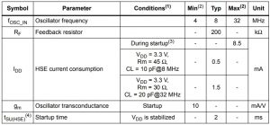
High-speed external clock generated from a crystal/ceramic resonatorThe high-speed external (HSE) clock can be supplied with a 4 to 32 MHz crystal/ceramic resonator oscillator. All the information given in this paragraph are based on design simulation results obtained with typical external components specified in Table 33. In the application, the resonator and the load capacitors have to be placed as close as possible to the oscillator pins in order to minimize output distortion and startup stabilization time. Refer to the crystal resonator manufacturer for more details on the resonator characteristics (frequency, package, accuracy).
Table 33. HSE oscillator characteristics
- Resonator characteristics given by the crystal/ceramic resonator manufacturer.
- Guaranteed by design, not tested in production.
- This consumption level occurs during the first 2/3 of the tSU(HSE) startup time.
- tSU(HSE) is the startup time measured from the moment it is enabled (by software) to a stabilized 8 MHz oscillation is reached. This value is measured for a standard crystal resonator and it can vary significantly with the crystal manufacture.
For CL1 and CL2, it is recommended to use high-quality external ceramic capacitors in the 5 pF to 20 pF range (Typ.), designed for high-frequency applications, and selected to match the requirements of the crystal or resonator (see Figure 16). CL1 and CL2 are usually the same size. The crystal manufacturer typically specifies a load capacitance which is the series combination of CL1 and CL2. PCB and MCU pin capacitance must be included (10 pF can be used as a rough estimate of the combined pin and board capacitance) when sizing CL1 and CL2.
Note: For information on selecting the crystal, refer to the application note AN2867 “Oscillator design guide for ST microcontrollers” available from the ST website www.st.com.
Figure 16. Typical application with an 8 MHz crystal
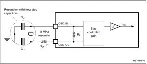
- REXT value depends on the crystal characteristics.
Low-speed external clock generated from a crystal resonatorThe low-speed external (LSE) clock can be supplied with a 32.768 kHz crystal resonator oscillator. All the information given in this paragraph are based on design simulation results obtained with typical external components specified in Table 34. In the application, the resonator and the load capacitors have to be placed as close as possible to the oscillator pins in order to minimize output distortion and startup stabilization time. Refer to the crystal resonator manufacturer for more details on the resonator characteristics (frequency,package, accuracy).
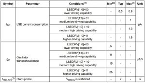
Table 34. LSE oscillator characteristics (fLSE = 32.768 kHz)
- Refer to the note and caution paragraphs below the table, and to the application note AN2867 “Oscillator design guide for ST microcontrollers”.
- Guaranteed by design, not tested in production.
- tSU(LSE) is the startup time measured from the moment it is enabled (by software) to a stabilized 32.768 kHz oscillation is reached. This value is measured for a standard crystal and it can vary significantly with the crystal manufacturer
Note: For information on selecting the crystal, refer to the application note AN2867 “Oscillator design guide for ST microcontrollers” available from the ST website www.st.com.
Figure 17. Typical application with a 32.768 kHz crystal
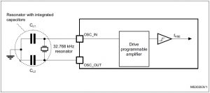
Note: An external resistor is not required between OSC32_IN and OSC32_OUT and it is forbidden to add one.
Internal clock source characteristicsThe parameters given in Table 35 are derived from tests performed under ambient temperature and supply voltage conditions summarized in Table 21: General operating conditions. The provided curves are characterization results, not tested in production.
High-speed internal (HSI) RC oscillator
Table 35. HSI oscillator characteristics(1)
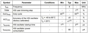
- VDDA = 3.3V, TA = -40 to 85°C unless otherwise specified
- Guaranteed by design, not tested in production.
- With user calibration
High-speed internal 14 MHz (HSI14) RC oscillator (dedicated to ADC)
Table 36. HSI14 oscillator characteristics(1)
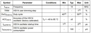
- VDDA = 3.3V, TA = -40 to 85°C unless otherwise specified
- Guaranteed by design, not tested in production.
Low-speed internal (LSI) RC oscillator
Table 37. LSI oscillator characteristics(1)
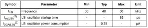
- VDDA = 3.3V, TA = -40 to 85°C unless otherwise specified.
- Guaranteed by design, not tested in production.
PLL characteristics
The parameters given in Table 38 are derived from tests performed under ambient temperature and supply voltage conditions summarized in Table 21: General operating conditions.
Table 38. PLL characteristics
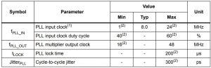
- Take care to use the appropriate multiplier factors to obtain PLL input clock values compatible with the range defined by fPLL_OUT.
- Guaranteed by design, not tested in production
Memory characteristics
Flash memoryThe characteristics are given at TA = -40 to 85 °C unless otherwise specified.
Table 39. Flash memory characteristics
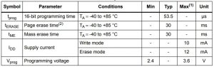
- Guaranteed by design, not tested in production.
- Page size is 1KB for STM32F030x4/6/8 devices and 2KB for STM32F030xC devices.
Table 40. Flash memory endurance and data retention
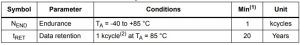
- Data based on characterization results, not tested in production.
- Cycling performed over the whole temperature range.
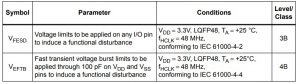
EMC characteristicsSusceptibility tests are performed on a sample basis during device characterization.
Functional EMS (electromagnetic susceptibility)While a simple application is executed on the device (toggling 2 LEDs through I/O ports). the device is stressed by two electromagnetic events until a failure occurs. The failure is indicated by the LEDs:
- Electrostatic discharge (ESD) (positive and negative) is applied to all device pins until a functional disturbance occurs. This test is compliant with the IEC 61000-4-2 standard.
- FTB: A Burst of Fast Transient voltage (positive and negative) is applied to VDD and VSS through a 100 pF capacitor, until a functional disturbance occurs. This test is compliant with the IEC 61000-4-4 standard.
A device reset allows normal operations to be resumed.
The test results are given in Table 41. They are based on the EMS levels and classes defined in application note AN1709.
Table 41. EMS characteristics
Designing hardened software to avoid noise problemsEMC characterization and optimization are performed at component level with a typical application environment and simplified MCU software. It should be noted that good EMC performance is highly dependent on the user application and the software in particular.Therefore it is recommended that the user applies EMC software optimization and prequalification tests in relation with the EMC level requested for his application.
Software recommendationsThe software flowchart must include the management of runaway conditions such as:
- Corrupted program counter
- Unexpected reset
- Critical Data corruption (control registers…)
Prequalification trialsMost of the common failures (unexpected reset and program counter corruption) can be reproduced by manually forcing a low state on the NRST pin or the Oscillator pins for 1 second.To complete these trials, ESD stress can be applied directly on the device, over the range of specification values. When unexpected behavior is detected, the software can be hardened to prevent unrecoverable errors occurring (see application note AN1015).
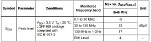
Electromagnetic Interference (EMI)The electromagnetic field emitted by the device are monitored while a simple application is executed (toggling 2 LEDs through the I/O ports). This emission test is compliant with IEC 61967-2 standard which specifies the test board and the pin loading.
Table 42. EMI characteristics
Electrical sensitivity characteristicsBased on three different tests (ESD, LU) using specific measurement methods, the device is stressed in order to determine its performance in terms of electrical sensitivity.
Electrostatic discharge (ESD)Electrostatic discharges (a positive then a negative pulse separated by 1 second) are applied to the pins of each sample according to each pin combination. The sample size depends on the number of supply pins in the device (3 parts × (n+1) supply pins). This test conforms to the JESD22-A114/C101 standard.
Table 43. ESD absolute maximum ratings
- Data based on characterization results, not tested in production
Static latch-upTwo complementary static tests are required on six parts to assess the latch-upperformance:
- A supply overvoltage is applied to each power supply pin.
- A current injection is applied to each input, output and configurable I/O pin.
These tests are compliant with EIA/JESD 78A IC latch-up standard.
Table 44. Electrical sensitivities
I/O current injection characteristicsAs a general rule, current injection to the I/O pins, due to external voltage below VSS or above VDDIOx (for standard, 3.3 V-capable I/O pins) should be avoided during normal product operation. However, in order to give an indication of the robustness of the microcontroller in cases when abnormal injection accidentally happens, susceptibility tests are performed on a sample basis during device characterization.
Functional susceptibility to I/O current injectionWhile a simple application is executed on the device, the device is stressed by injecting current into the I/O pins programmed in floating input mode. While current is injected into the I/O pin, one at a time, the device is checked for functional failures. The failure is indicated by an out of range parameter: ADC error above a certain limit (higher than 5 LSB TUE), out of conventional limits of induced leakage current on adjacent pins (out of the -5 μA/+0 μA range) or other functional failure (for example reset occurrence or oscillator frequency deviation).The characterization results are given in Table 45.Negative induced leakage current is caused by negative injection and positive induced leakage current is caused by positive injection.
Table 45. I/O current injection susceptibility
I/O port characteristics
General input/output characteristicsUnless otherwise specified, the parameters given in Table 46 are derived from tests performed under the conditions summarized in Table 21: General operating conditions. All I/Os are designed as CMOS- and TTL-compliant (except BOOT0).
Table 46. I/O static characteristics
- Data based on design simulation only. Not tested in production.
- The leakage could be higher than the maximum value, if negative current is injected on adjacent pins. Refer to Table 45: I/O current injection susceptibility.
- To sustain a voltage higher than VDDIOx + 0.3 V, the internal pull-up/pull-down resistors must be disabled.
- Pull-up and pull-down resistors are designed with a true resistance in series with a switchable PMOS/NMOS. This PMOS/NMOS contribution to the series resistance is minimal (~10% order).
All I/Os are CMOS- and TTL-compliant (no software configuration required). Their characteristics cover more than the strict CMOS-technology or TTL parameters. The coverage of these requirements is shown in Figure 18 for standard I/Os, and in Figure 19 for 5 V tolerant I/Os. The following curves are design simulation results, not tested in production.
Figure 18. TC and TTa I/O input characteristics
Figure 19. Five volt tolerant (FT and FTf) I/O input characteristics
Output driving currentThe GPIOs (general purpose input/outputs) can sink or source up to +/-8 mA, and sink or source up to +/- 20 mA (with a relaxed VOL/VOH).In the user application, the number of I/O pins which can drive current must be limited to respect the absolute maximum rating specified in Section 6.2:
- The sum of the currents sourced by all the I/Os on VDDIOx, plus the maximum consumption of the MCU sourced on VDD, cannot exceed the absolute maximum rating ΣIVDD (see Table 18: Voltage characteristics).
- The sum of the currents sunk by all the I/Os on VSS, plus the maximum consumption of the MCU sunk on VSS, cannot exceed the absolute maximum rating ΣIVSS (see Table 18: Voltage characteristics).
Output voltage levelsUnless otherwise specified, the parameters given in the table below are derived from tests performed under the ambient temperature and supply voltage conditions summarized in Table 21: General operating conditions. All I/Os are CMOS- and TTL-compliant (FT, TTa or TC unless otherwise specified).
Table 47. Output voltage characteristics(1)
- The IIO current sourced or sunk by the device must always respect the absolute maximum rating specified in Table 18: Voltage characteristics, and the sum of the currents sourced or sunk by all the I/Os (I/O ports and control pins) must always respect the absolute maximum ratings ΣIIO.
- Data based on characterization results. Not tested in production.
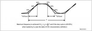
Input/output AC characteristicsThe definition and values of input/output AC characteristics are given in Figure 20 and Table 48, respectively.Unless otherwise specified, the parameters given are derived from tests performed under the ambient temperature and supply voltage conditions summarized in Table 21: General operating conditions.
Table 48. I/O AC characteristics(1)(2)
- The I/O speed is configured using the OSPEEDRx[1:0] bits. Refer to the STM32F0xxxx RM0360 reference manual for a description of GPIO Port configuration register.
- Guaranteed by design, not tested in production.
- The maximum frequency is defined in Figure 20.
- When Fm+ configuration is set, the I/O speed control is bypassed. Refer to the STM32F0xxxx reference manual RM0360 for a detailed description of Fm+ I/O configuration.
Figure 20. I/O AC characteristics definition
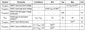
NRST pin characteristicsThe NRST pin input driver uses the CMOS technology. It is connected to a permanent pullup resistor, RPU.
Unless otherwise specified, the parameters given in the table below are derived from tests performed under the ambient temperature and supply voltage conditions summarized in Table 21: General operating conditions.
Table 49. NRST pin characteristics
- Data based on design simulation only. Not tested in production.
- The pull-up is designed with a true resistance in series with a switchable PMOS. This PMOS contribution to the series resistance is minimal (~10% order).
- Data based on design simulation only. Not tested in production.
Figure 21. Recommended NRST pin protection
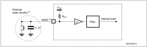
- The external capacitor protects the device against parasitic resets.
- The user must ensure that the level on the NRST pin can go below the VIL(NRST) max level specified in Table 49: NRST pin characteristics. Otherwise the reset will not be taken into account by the device.
12-bit ADC characteristicsUnless otherwise specified, the parameters given in Table 50 are preliminary values derived from tests performed under ambient temperature, fPCLK frequency and VDDA supply voltage conditions summarized in Table 21: General operating conditions.
Table 50. ADC characteristics
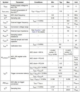
Note: It is recommended to perform a calibration after each power-up.
- During conversion of the sampled value (12.5 x ADC clock period), an additional consumption of 100 μA on IDDA and 60 μA on IDD should be taken into account.
- Guaranteed by design, not tested in production.
Equation 1: RAIN max formula
The formula above (Equation 1) is used to determine the maximum external impedance allowed for an error below 1/4 of LSB. Here N = 12 (from 12-bit resolution).
Table 51. RAIN max for fADC = 14 MHz
- Guaranteed by design, not tested in production.
Table 52. ADC accuracy(1)(2)(3)
- ADC DC accuracy values are measured after internal calibration.
- ADC Accuracy vs. Negative Injection Current: Injecting negative current on any of the standard (non-robust) analog input pins should be avoided as this significantly reduces the accuracy of the conversion being performed on another analog input. It is recommended to add a Schottky diode (pin to ground) to standard analog pins which may potentially inject negative current.Any positive injection current within the limits specified for IINJ(PIN) and ΣIINJ(PIN) in Section 6.3.14 does not affect the ADC accuracy.
- Better performance may be achieved in restricted VDDA, frequency and temperature ranges.
- Data based on characterization results, not tested in production.
Figure 22. ADC accuracy characteristics
Figure 23. Typical connection diagram using the ADC
- Refer to Table 50: ADC characteristics for the values of RAIN, RADC and CADC.
- Cparasitic represents the capacitance of the PCB (dependent on soldering and PCB layout quality) plus the pad capacitance (roughly 7 pF). A high Cparasitic value will downgrade conversion accuracy. To remedy this, fADC should be reduced.
General PCB design guidelinesPower supply decoupling should be performed as shown in Figure 12: Power supply scheme. The 10 nF capacitor should be ceramic (good quality) and it should be placed as close as possible to the chip.
Temperature sensor characteristics
Table 53. TS characteristics
- Guaranteed by design, not tested in production.
- Measured at VDDA = 3.3 V ± 10 mV. The V30 ADC conversion result is stored in the TS_CAL1 byte. Refer to Table 3: Temperature sensor calibration values
Timer characteristicsThe parameters given in the following tables are guaranteed by design.Refer to Section 6.3.14: I/O port characteristics for details on the input/output alternate function characteristics (output compare, input capture, external clock, PWM output).
Table 54. TIMx characteristics
Table 55. IWDG min/max timeout period at 40 kHz (LSI)(1)
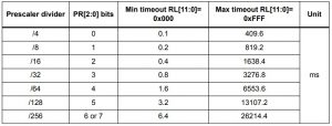
- These timings are given for a 40 kHz clock but the microcontroller internal RC frequency can vary from 30 to 60 kHz. Moreover, given an exact RC oscillator frequency, the exact timings still depend on the phasing of the APB interface clock versus the LSI clock so that there is always a full RC period of uncertainty.
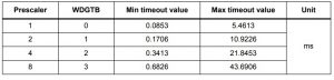
Table 56. WWDG min/max timeout value at 48 MHz (PCLK)
Communication interfaces
I2C interface characteristics
The I2C interface meets the timings requirements of the I2C-bus specification and user manual rev. 03 for:
- Standard-mode (Sm): with a bit rate up to 100 kbit/s
- Fast-mode (Fm): with a bit rate up to 400 kbit/s
- Fast-mode Plus (Fm+): with a bit rate up to 1 Mbit/s.
The I2C timings requirements are guaranteed by design when the I2C peripheral is properly configured (refer to Reference manual).The SDA and SCL I/O requirements are met with the following restrictions: the SDA and SCL I/O pins are not “true” open-drain. When configured as open-drain, the PMOS connected between the I/O pin and VDDIOx is disabled, but is still present. Only FTf I/O pins support Fm+ low level output current maximum requirement. Refer to Section 6.3.14: I/O port characteristics for the I2C I/Os characteristics.All I2C SDA and SCL I/Os embed an analog filter. Refer to the table below for the analog filter characteristics:
Table 57. I2C analog filter characteristics(1)
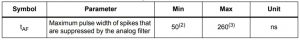
- Guaranteed by design, not tested in production.
- Spikes with widths below tAF(min) are filtered.
- Spikes with widths above tAF(max) are not filtered
SPI characteristicsUnless otherwise specified, the parameters given in Table 58 for SPI are derived from tests performed under the ambient temperature, fPCLKx frequency and supply voltage conditions summarized in Table 21: General operating conditions.Refer to Section 6.3.14: I/O port characteristics for more details on the input/output alternate function characteristics. Unless otherwise specified, the parameters given in Table 58 for SPI are derived from tests performed under the ambient temperature, fPCLKx frequency and supply voltage conditions summarized in Table 21: General operating conditions.Refer to Section 6.3.14: I/O port characteristics for more details on the input/output alternate function characteristics.
Table 58. SPI characteristics(1)
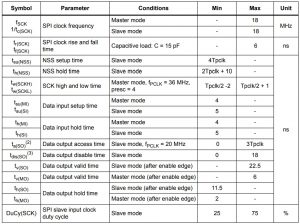
- Data based on characterization results, not tested in production.
- Min time is for the minimum time to drive the output and the max time is for the maximum time to validate the data.
- Min time is for the minimum time to invalidate the output and the max time is for the maximum time to put the data in Hi-Z
Figure 24. SPI timing diagram – slave mode and CPHA = 0
Figure 25. SPI timing diagram – slave mode and CPHA = 1
- Measurement points are done at CMOS levels: 0.3 VDD and 0.7 VDD
Figure 26. SPI timing diagram – master mode
 Measurement points are done at CMOS levels: 0.3 VDD and 0.7 VDD
 Measurement points are done at CMOS levels: 0.3 VDD and 0.7 VDD
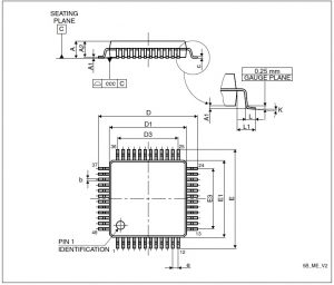
Package characteristics
Package mechanical data
In order to meet environmental requirements, ST offers these devices in different grades of ECOPACK® packages, depending on their level of environmental compliance. ECOPACK® specifications, grade definitions and product status are available at: www.st.com. ECOPACK® is an ST trademark.
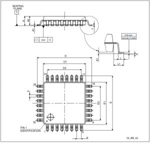
Figure 27. LQFP64 – 10 x 10 mm 64 pin low-profile quad flat package outline
- Drawing is not to scale.
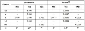
Table 59. LQFP64 – 10 x 10 mm low-profile quad flat package mechanical data
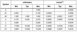
- Values in inches are converted from mm and rounded to 4 decimal digits
Figure 28. LQFP64 recommended footprint
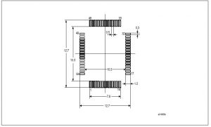
- Dimensions are in millimeters
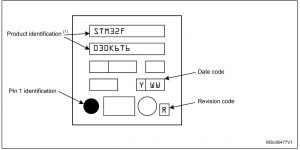
Device marking for LQFP64The following figure shows the device marking for the LQFP64 package.
Figure 29. LQFP64 marking example (package top view)
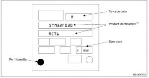
- Parts marked as “ES”, “E” or accompanied by an Engineering Sample notification letter, are not yet qualified and therefore not yet ready to be used in production and any consequences deriving from such usage will not be at ST charge. In no event, ST will be liable for any customer usage of these engineering samples in production. ST Quality has to be contacted prior to any decision to use these Engineering samples to run qualification activity.
Figure 30. LQFP48 – 7 mm x 7 mm, 48 pin low-profile quad flat package outline
- Drawing is not to scale
Table 60. LQFP48 – 7 mm x 7 mm low-profile quad flat package mechanical data
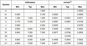
Table 60. LQFP48 – 7 mm x 7 mm low-profile quad flat package mechanical data (continued)
- Values in inches are converted from mm and rounded to 4 decimal digits.
Figure 31. LQFP48 recommended footprint

- Dimensions are in millimeters.
Device marking for LQFP48The following figure shows the device marking for the LQFP48 package.
Figure 32. LQFP48 marking example (package top view)
- Parts marked as “ES”, “E” or accompanied by an Engineering Sample notification letter, are not yet qualified and therefore not yet ready to be used in production and any consequences deriving from such usage will not be at ST charge. In no event, ST will be liable for any customer usage of these engineering samples in production. ST Quality has to be contacted prior to any decision to use these Engineering samples to run qualification activity.
Figure 33. LQFP32 – 7 x 7mm 32-pin low-profile quad flat package outline
- Drawing is not to scale
Table 61. LQFP32 – 7 x 7mm 32-pin low-profile quad flat package mechanical d
Table 61. LQFP32 – 7 x 7mm 32-pin low-profile quad flat package mechanical data (continued)
- Values in inches are converted from mm and rounded to 4 decimal digits.
Figure 34. LQFP32 recommended footprint
- Drawing is not to scale.
- Dimensions are in millimeters.
Device marking for LQFP32The following figure shows the device marking for the LQFP32 package.
Figure 35. LQFP32 marking example (package top view)

- Parts marked as “ES”, “E” or accompanied by an Engineering Sample notification letter, are not yet qualified and therefore not yet ready to be used in production and any consequences deriving from such usage will not be at ST charge. In no event, ST will be liable for any customer usage of these engineering samples in production. ST Quality has to be contacted prior to any decision to use these Engineering samples to run qualification activity
Figure 36. TSSOP20 – 20-pin thin shrink small outline
- Drawing is not to scale.
Table 62. TSSOP20 – 20-pin thin shrink small outline package mechanical d
- Values in inches are converted from mm and rounded to 4 decimal digits.
- Dimension “D” does not include mold flash, protrusions or gate burrs. Mold flash, protrusions or gate burrs shall not exceed 0.15mm per side.
- Dimension “E1” does not include interlead flash or protrusions. Interlead flash or protrusions shall not exceed 0.25mm per side.
Figure 37. TSSOP20 recommended footprint
Dimensions are in millimeters.Device marking for TSSOP20The following figure shows the device marking for the TSSOP20 package.
Figure 38. TSSOP20 marking example (package top view)
- Parts marked as “ES”, “E” or accompanied by an Engineering Sample notification letter, are not yet qualified and therefore not yet ready to be used in production and any consequences deriving from such usage will not be at ST charge. In no event, ST will be liable for any customer usage of these engineering samples in production. ST Quality has to be contacted prior to any decision to use these Engineering samples to run qualification activity
 Parts marked as “ES”, “E” or accompanied by an Engineering Sample notification letter, are not yet qualified and therefore not yet ready to be used in production and any consequences deriving from such usage will not be at ST charge. In no event, ST will be liable for any customer usage of these engineering samples in production. ST Quality has to be contacted prior to any decision to use these Engineering samples to run qualification activity
Thermal characteristics
The maximum chip junction temperature (TJmax) must never exceed the values given in Table 21: General operating conditions.
The maximum chip-junction temperature, TJ max, in degrees Celsius, may be calculated using the following equation:
TJ max = TA max + (PD max x ΘJA)
Where:
- TA max is the maximum ambient temperature in °C,
- ΘJA is the package junction-to-ambient thermal resistance, in °C/W,
- PD max is the sum of PINT max and PI/O max (PD max = PINT max + PI/Omax),
- PINT max is the product of IDD and VDD, expressed in Watts. This is the maximum chip internal power.
PI/O max represents the maximum power dissipation on output pins where:
PI/O max = Σ (VOL × IOL) + Σ ((VDD – VOH) × IOH),
taking into account the actual VOL / IOL and VOH / IOH of the I/Os at low and high level in the application.
Table 63. Package thermal characteristics
Reference document
JESD51-2 Integrated Circuits Thermal Test Method Environment Conditions – Natural Convection (Still Air). Available from www.jedec.org
Part numbering
For a list of available options (memory, package, and so on) or for further information on any aspect of this device, please contact your nearest ST sales office.
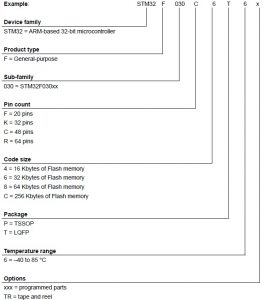
Revision history
Table 65. Document revision history
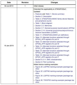
IMPORTANT NOTICE – PLEASE READ CAREFULLYSTMicroelectronics NV and its subsidiaries (“ST”) reserve the right to make changes, corrections, enhancements, modifications, and improvements to ST products and/or to this document at any time without notice. Purchasers should obtain the latest relevant information on ST products before placing orders. ST products are sold pursuant to ST’s terms and conditions of sale in place at the time of order acknowledgement.
Purchasers are solely responsible for the choice, selection, and use of ST products and ST assumes no liability for application assistance or the design of Purchasers’ products.
No license, express or implied, to any intellectual property right is granted by ST herein.
Resale of ST products with provisions different from the information set forth herein shall void any warranty granted by ST for such product.
ST and the ST logo are trademarks of ST. All other product or service names are the property of their respective owners.
Information in this document supersedes and replaces information previously supplied in any prior versions of this document.
© 2015 STMicroelectronics – All rights reserved
life.augmented Value-line ARM Operation Datasheet STM32F030x4, STM32F030x6, STM32F030x8, STM32F030xC – life.augmented Value-line ARM Operation Datasheet STM32F030x4, STM32F030x6, STM32F030x8, STM32F030xC –
[xyz-ips snippet=”download-snippet”]