
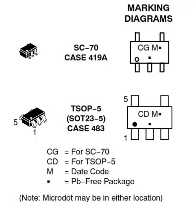
NS5B1G385
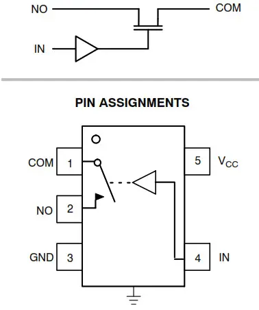
Analog Switch, Single SPST, (NO) Normally OpenThe NS5B1G385 is Single Pole Single Throw (SPST) high-speed TTL-compatible switch. The low resistance and capacitance characteristics of this switch make it ideal for low-distortion audio, video, and data routing applications. The switch has a normally open logic configuration meaning the switch is on (NO connected to COM) when IN is high. These switches are available in 5-pin SC-70 and 5 -pin TSOP-5 (SOT23-5) packages for operation over the industrial (-40°C to +85°C) temperature range.
Features
- VCC Operating Range: 2.0 V to 5.5 V
- Low On Resistance : RON: 4.0 W Typical @ VCC = 4.5 V
- Minimal Propagation Delay : tpd < 0.5 ns
- Control Input Compatible with TTL Levels
- ESD Performance: Human Body Model > ±2 kV
- 5-Pin SC-70 or 5-Pin TSOP-5 Packages Available
- These are Pb-Free Devices
Typical Applications
- Audio, Video, and High-Speed Data Switching
- Mobile Phones
- Portable Devices
- Desktop & Notebook Computing
PIN SESCRIPTION
| PIN # | Name | Direction | Description |
| 1 | COM | I/O | Common Signal Line |
| 2 | NO | I/O | Normally Open Signal Line |
| 3 | GND | Input | Ground |
| 4 | IN | Input | Control Signal Line |
| 5 | VCC | Input | Voltage Supply |
TRUTH TABLE
| IN Control Input | Function |
| L | NO Disconnected from COM |
| H | NO Connected to COM |
MAXIMUM RATINGS
| Symbol | Pins | Rating | Value | Condition | Unit |
| VCC | VCC | Positive DC Supply Voltage | -0.5 to +7.0 | V | |
| Vls | NO or COM | Analog Signal Voltage | -0.5 to Vcc + 0.5 | V | |
| VIN | IN | Control Input Voltage | -0.5 to +7.0 | V | |
| liS_CON | NO or COM | Analog Signal Continuous Current | ± 300 | Closed Switch | mA |
| ‘ism( | NO or COM | Analog Signal Peak Current | ± 500 | 10% Duty Cycle | mA |
| liN | IN | Control Input Current | ± 20 | mA | |
| TSTG | Storage Temperature Range | -65 to 150 | ºC |
Stresses exceeding Maximum Ratings may damage the device. Maximum Ratings are stress ratings only. Functional operation above the Recommended Operating Conditions is not implied. Extended exposure to stresses above the Recommended Operating Conditions may affect device reliability.
RECOMMENDED OPERATING CONDITIONS
| Symbol | Pins | Parameter | Value | Condition | Unit |
| VCC | VCC | Positive DC Supply Voltage | 2.0 to 5.5 | V | |
| Vis | NO or COM | Analog Signal Voltage | GND to Vcc | V | |
| VIN | IN | Control Input Voltage | GND to 5.5 | V | |
| TA | Operating Temperature Range | -40 to +85 | ºC | ||
| tr, tr | Input Rise or Fall Time | 20 | VCC = 3.3 V | nsN | |
| 10 | VCC = 5.0 V |
Minimum and maximum values are guaranteed through test or design across the Recommended Operating Conditions, where applicable. Typical values are listed for guidance only and are based on the particular conditions listed for each section, where applicable. These conditions are valid for all values found in the characteristics tables unless otherwise specified in the test conditions.
ESD PROTECTION
| Pins | Description | Minimum Voltage |
| All Pins | Human Body Model | 2 kV |
DC ELECTRICAL CHARACTERISTICS CONTROL INPUT (Typical: T = 25°C)
| Symbol | Pins | Parameter | Test Conditions | VCC(V) | -40°C to +85°C | Unit | |
| Min | Typ | Max | |||||
| VIH | IN | Control Input High | 4.5 – 5.5 | 2.0 | V | ||
| VIL | IN | Control Input Low | 4.5 – 5.5 | 0.8 | V | ||
| IIN | IN | Control Input Leakage | 0 s VIN s VCC | 5.0 | ±0.1 | ±0.5 | itA |
SUPPLY CURRENT AND LEAKAGE (Typical: T = 25°C)
| Symbol | Pins | Parameter | Test Conditions | VCC(V) | -40°C to +85°C | Unit | |
| Min | Typ | Max | |||||
| INO (OFF) | NO | OFF State Leakage | VIN = VIL or Vitt VNO = 1.0 VVoom = 4.5 V | 6. | ±10 | ±100 | nA |
| ‘COM (OFF) | COM | OFF State Leakage | VIN = VII_ or VIH Vt,i0 = 4.5 VVow = 1.0 V | 6. | 110 | ±100 | nA |
| ICC | \Jim | Quiescent Supply | VIN and Vis = VCC or GND ID = 0 A | 2.0 – 5.5 | ±0.1 | ±1.0 | μA |
| TOFF | IN | Power Off Leakage | VIN = 5.5 V or GND | 0 | 11. | ±1.0 | μA |
ON RESISTANCE (Typical: T = 25°C)
| Symbol | Pins | Parameter | Test Conditions | VCC (V) | −40 ºC to +85 ºC |
Unit |
|
|
Min |
Typ |
Max |
|||||
|
RON |
NO, COM | ON Resistance | VIS = 0 V, ION = 30 mAVIS = 0 V, ION = 64 mAVIS = 2.4 V, ION = 15 mA | 4.54.54.5 | 4.04.011.5 |
7.07.015 |
Ω |
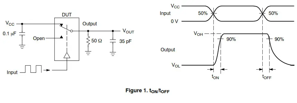
AC ELECTRICAL CHARACTERISTICSTIMING/FREQUENCY (Typical: T = 25°C, RL = 50 Ω, CL = 35 pF, f = 1 MHz)
| Symbol | Pins | Parameter | Test Conditions | VCC(V) | -40°C to 4-85°C | Unit |
| Min | Typ | Max | ||||
| tON | IN to NO | Turn On Time | As Above, Figures 1 and 2 | 4.5 | 6.0 | ns |
| tOFF | IN to NO | Turn Off Time | As Above, Figures 1 and 2 | 4.5 | 2.0 | ns |
| tPD | NO to COM | Propagation Delay | As Above | 4.5 | 0.5 | ns |
| BW | -3dB Bandwidth | CL = 5 pF, Figures 3 and 4 | 4.5 | 330 | MHz |
CAPACITANCE (Typical: T = 25°C, RL = 50 , CL = 5 pF, f = 1 MHz)
| Symbol | Pins | Parameter | Test Conditions | VCC(V) | -40°C to 4-85°C | Unit |
| Min | Typ | Max | ||||
| CIN | IN | Control Input | 0 V | 2. | pF | |
| CON | NO to COM | Through Switch | VIN = OV | 4.5 V | 12 | pF |
| COFF | NO | Unselected Port | Vis = 4.5 V, VIN = 4.5 V | 4.5 V | 4. | pF |
DEVICE ORDERING INFORMATION
| Device Order Number | Package Type | Tape & Reel Sizet |
| NS5B1G385DFT2G | SC-70 (Pb-Free) | 3000 / Tape & Reel |
| NS5B1G385DTT1G | TSOP-5 (Pb-Free) | 3000 / Tape & Reel |
For information on tape and reel specifications, including part orientation and tape sizes, please refer to our Tape and Reel Packaging Specifications Brochure, BRD8011/D.
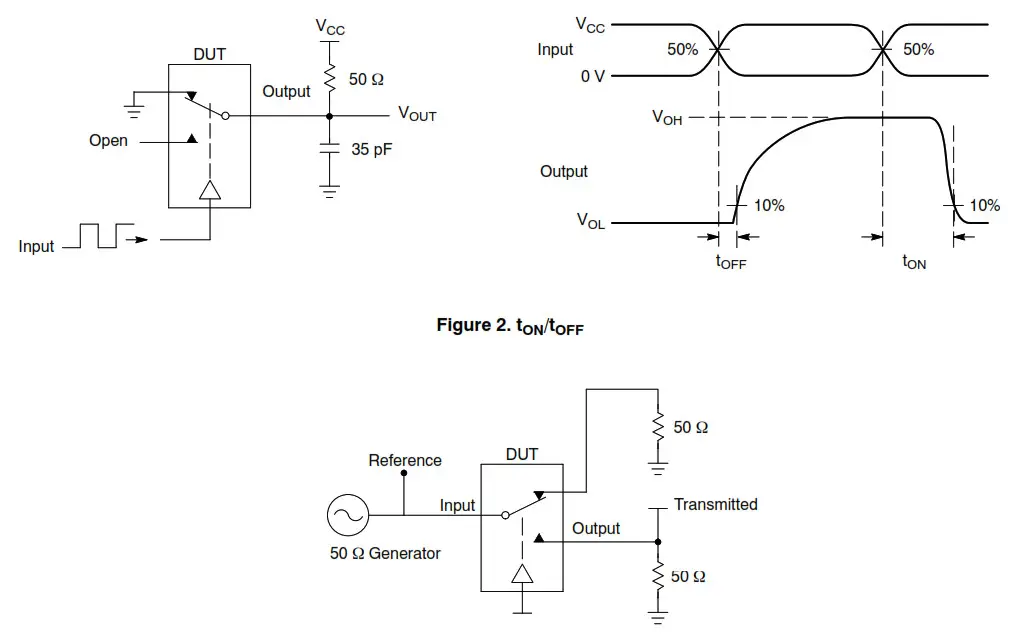
Channel switch control/s test socket is normalized. Off isolation is measured across an off channel. On loss is the bandwidth of an On switch. VISO, Bandwidth and VONL are independent of the input signal direction.VISO = Off Channel Isolation = 20 Log ![]() for VIN at 100 kHzVONL = On Channel Loss = 20 Log
for VIN at 100 kHzVONL = On Channel Loss = 20 Log ![]() for VIN at 100 kHz to 50 MHz
for VIN at 100 kHz to 50 MHz
Bandwidth (BW) = the frequency 3 dB below VONLVCT = Use VISO setup and test to all other switch analog input/outputs terminated with 50 W
Figure 3. Off Channel Isolation/On Channel Loss (BW)/Crosstalk (On Channel to Off Channel)/VONL
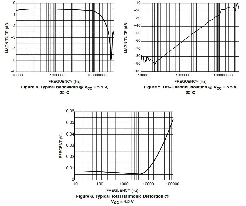 Figure 4. Typical Bandwidth @ VCC = 5.5 V, 255C
MECHANICAL CASE OUTLINE
PACKAGE DIMENSIONS
SC-88A (SC-70-5/SOT-353)CASE 419A-02ISSUE L
![]() SCALE 2:1
SCALE 2:1
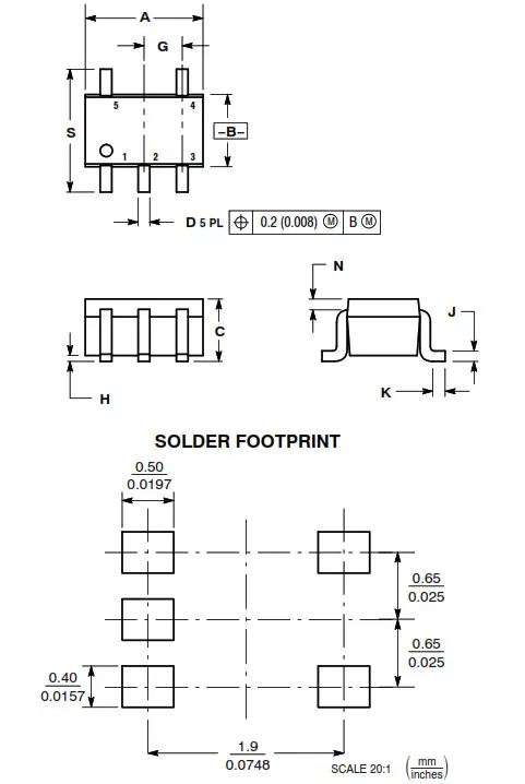
NOTES:
- DIMENSIONING AND TOLERANCING PER ANSI Y14.5M, 1982.
- CONTROLLING DIMENSION: INCH.
- 419A-01 OBSOLETE. NEW STANDARD 419A-02.
- DIMENSIONS A AND B DO NOT INCLUDE MOLD FLASH, PROTRUSIONS, OR GATE BURRS.
| DIM | INCHES | MILLIMETERS | ||
| MIN | MAX | MIN | MAX | |
| A | 0.071 | 0.087 | 1.80 | 2.20 |
| B | 0.045 | 0.053 | 1. | 1. |
| C | 0.031 | 0.043 | 0.80 | 1.10 |
| D | 0.004 | 0.012 | 0.10 | 0.30 |
| G | 0.026 BSC | 0.65 BSC | ||
| H | 0.004 | 0.10 | ||
| J | 0.004 | 0.010 | 0.10 | 0.25 |
| K | 0.004 | 0.012 | 0.10 | 0.30 |
| N | 0.008 REF | 0.20 REF | ||
| S | 0.079 | 0.087 | 2.00 | 2.20 |
GENERIC MARKING DIAGRAM*
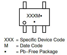
(Note: Microdot may be in either location)*This infomration is generic. Please refer to device data sheet for actual part marking.
| STYLE 1: | STYLE 2: | STYLE 3: | STYLE 4: | STYLE 5: |
| PIN 1. BASE2. EMITTER3. BASE4. COLLECTOR5. COLLECTOR | PIN 1. ANODE2. EMITTER3. BASE4. COLLECTOR5. CATHODE | PIN 1. ANODE 12. N/C3. ANODE 24. CATHODE 25. CATHODE 1 | PIN 1. SOURCE 12. DRAIN 1/23. SOURCE 14. GATE 15. GATE 2 | PIN 1. CATHODE2. COMMON ANODE3. CATHODE 24. CATHODE 35. CATHODE 4 |
| STYLE 6: | STYLE 7: | STYLE 8: | STYLE 9: | |
| PIN 1. EMITTER 22. BASE 23. EMITTER 14. COLLECTOR5. COLLECTOR 2/BASE 1 | PIN 1. BASE2. EMITTER3. BASE4. COLLECTOR5. COLLECTOR | PIN 1. CATHODE2. COLLECTOR3. N/C4. BASE5. EMITTER | PIN 1. ANODE2. CATHODE3. ANODE4. ANODE5. ANODE |
| DOCUMENT NUMBER: | 98ASB42984B | Electronic versions are uncontrolled except whenaccessed directly from the Document Repository. Printed versions are uncontrolled except when stamped“CONTROLLED COPY’ in red. |
| STATUS: | ON SEMICONDUCTOR STANDARD | |
| NEW STANDARD: | ||
| DESCRIPTION: | SC-88A (SC-70-5/SOT-353) | PAGE 1 OF 2 |
| ON Semlconductor® |
DOCUMENT NUMBER:98ASB42984B | |
| PAGE 2 OF 2 | ||
| ISSUE | REVISION | DATE |
| C | CONVERTED FROM PAPER DOCUMENT TO ELECTRONIC. REQ. BY N LAFEBRE. | 20 JUN 1998 |
| D | CONVERTED FROM MOTOROLA TO ON SEMICONDUCTOR. ADDED STYLE 5. REQ. BY E. KIM. | 24 JUL 2000 |
| E | ADDED STYLES 6 & 7. REQ. BY S. BACHMAN. | 03 AUG 2000 |
| F | DELETED DIMENSION V, WAS 0.3−0.44MM/0.012−0.016IN. REQ. BY G. KWONG. | 14 JUN 2001 |
| G | ADDED STYLE 8, REQ. BY S. CHANG; ADDED STYLE 9, REQ. BY S. BACHMAN; ADDED NOTE 4, REQ. BY S. RIGGS | 25 JUN 2003 |
| H | CHANGED STYLE 6. REQ. BY C. LIM | 28 APR 2005 |
| J | CHANGED TITLE DESCRIPTION. REQ. BY B. LOFTS. | 31 AUG 2005 |
| K | CORRECTED TITLE AND DESCRIPTION TO SC−88A (SC−70−5/SOT−353). CORRECTED MARKING DIAGRAM. REQ. BY D. TRUHITTE. | 13 JUL 2010 |
| L | ADDED SOLDER FOOTPRINT. REQ. BY I. MARIANO. | 17 JAN 2013 |
ON Semiconductor ![]() and are registered trademarks of Semiconductor Components Industries, LLC (SCILLC). SCILLC reserves the right to make changes without further notice to any products herein. SCILLC makes no warranty, representation or guarantee regarding the suitability of its products for any particular purpose, nor does SCILLC assume any liability arising out of the application or use of any product or circuit, and specifically disclaims any and all liability, including without limitation special, consequential or incidental damages. “Typical” parameters which may be provided in SCILLC data sheets and/or specifications can and do vary in different applications and actual performance may vary over time. All operating parameters, including “Typicals” must be validated for each customer application by customer’s technical experts. SCILLC does not convey any license under its patent rights nor the rights of others. SCILLC products are not designed, intended, or authorized for use as components in systems intended for surgical implant into the body, or other applications intended to support or sustain life, or for any other application in which the failure of the SCILLC product could create a situation where personal injury or death may occur. Should Buyer purchase or use SCILLC products for any such unintended or unauthorized application, Buyer shall indemnify and hold SCILLC and its officers, employees, subsidiaries, affiliates, and distributors harmless against all claims, costs, damages, and expenses, and reasonable attorney fees arising out of, directly or indirectly, any claim of personal injury or death associated with such unintended or unauthorized use, even if such claim alleges that SCILLC was negligent regarding the design or manufacture of the part. SCILLC is an Equal Opportunity/Affirmative Action Employer. This literature is subject to all applicable copyright laws and is not for resale in any manner.
and are registered trademarks of Semiconductor Components Industries, LLC (SCILLC). SCILLC reserves the right to make changes without further notice to any products herein. SCILLC makes no warranty, representation or guarantee regarding the suitability of its products for any particular purpose, nor does SCILLC assume any liability arising out of the application or use of any product or circuit, and specifically disclaims any and all liability, including without limitation special, consequential or incidental damages. “Typical” parameters which may be provided in SCILLC data sheets and/or specifications can and do vary in different applications and actual performance may vary over time. All operating parameters, including “Typicals” must be validated for each customer application by customer’s technical experts. SCILLC does not convey any license under its patent rights nor the rights of others. SCILLC products are not designed, intended, or authorized for use as components in systems intended for surgical implant into the body, or other applications intended to support or sustain life, or for any other application in which the failure of the SCILLC product could create a situation where personal injury or death may occur. Should Buyer purchase or use SCILLC products for any such unintended or unauthorized application, Buyer shall indemnify and hold SCILLC and its officers, employees, subsidiaries, affiliates, and distributors harmless against all claims, costs, damages, and expenses, and reasonable attorney fees arising out of, directly or indirectly, any claim of personal injury or death associated with such unintended or unauthorized use, even if such claim alleges that SCILLC was negligent regarding the design or manufacture of the part. SCILLC is an Equal Opportunity/Affirmative Action Employer. This literature is subject to all applicable copyright laws and is not for resale in any manner.
MECHANICAL CASE OUTLINE
PACKAGE DIMENSIONS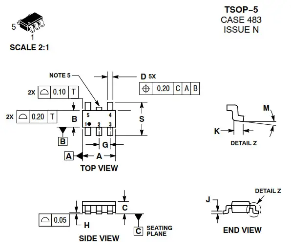
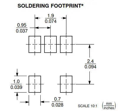 *For additional information on our Pb−Free strategy and soldering details, please download the ON Semiconductor Soldering and Mounting Techniques Reference Manual, SOLDERRM/D.
NOTES:
- DIMENSIONING AND TOLERANCING PER ASME Y14.5M, 1994.
- CONTROLLING DIMENSION: MILLIMETERS.
- MAXIMUM LEAD THICKNESS INCLUDES LEAD FINISH THICKNESS. MINIMUM LEAD THICKNESS IS THE MINIMUM THICKNESS OF BASE MATERIAL.
- DIMENSIONS A AND B DO NOT INCLUDE MOLD FLASH, PROTRUSIONS, OR GATE BURRS. MOLD FLASH, PROTRUSIONS, OR GATE BURRS SHALL NOT EXCEED 0.15 PER SIDE. DIMENSION A.
- OPTIONAL CONSTRUCTION: AN ADDITIONAL TRIMMED LEAD IS ALLOWED IN THIS LOCATION. TRIMMED LEAD NOT TO EXTEND MORE THAN 0.2 FROM BODY.
DIM MILLIMETERS MIN MAX A 3. 3. B 1. 2. C 0.90 1.10 D 0.25 0.50 G 0.95 BSC H 0.01 0.10 J 0.10 0.26 K 0.20 0.60 M 0º 10º S 2.50 3.00
GENERIC MARKING DIAGRAM*
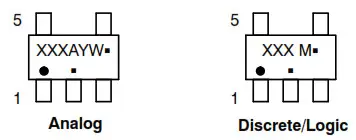
| XXX = Specific Device CodeA = Assembly LocationY = YearW = Work Week• = Pb−Free Package | XXX = Specific Device CodeM = Date Code• = Pb−Free Package |
(Note: Microdot may be in either location)*This information is generic. Please refer to device data sheet for actual part marking. Pb-Free indicator, “G” or microdot ” • “, may or may not be present.
| DOCUMENT NUMBER: | 98ARB18753C | Electronic versions are uncontrolled except when accessed directly from the Document Repository.Printed versions are uncontrolled except when stamped CONTROLLED COPY” in red. |
| DESCRIPTION: | TSOP−5 | PAGE 1 OF 1 |
ON Semiconductor ![]() reserves the right to make changes without further notice to any products herein. ON Semiconductor makes no warranty, representation or guarantee regarding the suitability of its products for any particular purpose, nor does ON Semiconductor assume any liability arising out of the application or use of any product or circuit, and specifically disclaims any and all liability, including without limitation special, consequential or incidental damages. ON Semiconductor does not convey any license under its patent rights nor the rights of others.
reserves the right to make changes without further notice to any products herein. ON Semiconductor makes no warranty, representation or guarantee regarding the suitability of its products for any particular purpose, nor does ON Semiconductor assume any liability arising out of the application or use of any product or circuit, and specifically disclaims any and all liability, including without limitation special, consequential or incidental damages. ON Semiconductor does not convey any license under its patent rights nor the rights of others.
ON Semiconductor and are trademarks of Semiconductor Components Industries, LLC dba ON Semiconductor or its subsidiaries in the United States and/or other countries. ON Semiconductor owns the rights to a number of patents, trademarks, copyrights, trade secrets, and other intellectual property. A listing of ON Semiconductor’s product/patent coverage may be accessed at www.onsemi.com/site/pdf/Patent-Marking.pdf. ON Semiconductor reserves the right to make changes without further notice to any products herein. ON Semiconductor makes no warranty, representation or guarantee regarding the suitability of its products for any particular purpose, nor does ON Semiconductor assume any liability arising out of the application or use of any product or circuit, and specifically disclaims any and all liability, including without limitation special, consequential or incidental damages. Buyer is responsible for its products and applications using ON Semiconductor products, including compliance with all laws, regulations and safety requirements or standards, regardless of any support or applications information provided by ON Semiconductor. “Typical” parameters which may be provided in ON Semiconductor data sheets and/or specifications can and do vary in different applications and actual performance may vary over time. All operating parameters, including “Typicals” must be validated for each customer application by customer’s technical experts. ON Semiconductor does not convey any license under its patent rights nor the rights of others. ON Semiconductor products are not designed, intended, or authorized for use as a critical component in life support systems or any FDA Class 3 medical devices or medical devices with a same or similar classification in a foreign jurisdiction or any devices intended for implantation in the human body. Should Buyer purchase or use ON Semiconductor products for any such unintended or unauthorized application, Buyer shall indemnify and hold ON Semiconductor and its officers, employees, subsidiaries, affiliates, and distributors harmless against all claims, costs, damages, and expenses, and reasonable attorney fees arising out of, directly or indirectly, any claim of personal injury or death associated with such unintended or unauthorized use, even if such claim alleges that ON Semiconductor was negligent regarding the design or manufacture of the part. ON Semiconductor is an Equal Opportunity/Affirmative Action Employer. This literature is subject to all applicable copyright laws and is not for resale in any manner.
PUBLICATION ORDERING INFORMATION
LITERATURE FULFILLMENT:Email Requests to: [email protected]ON Semiconductor Website: www.onsemi.com
TECHNICAL SUPPORTNorth American Technical Support: Voice Mail: 1 800-282-9855 Toll Free USA/CanadaPhone: 011 421 33 790 2910
Europe, Middle East and Africa Technical Support: Phone: 00421 33 790 2910 For additional information, please contact your local Sales Representative
 report this ad
Mouser ElectronicsAuthorized DistributorClick to View Pricing, Inventory, Delivery & Lifecycle Information:ON Semiconductor:NS5B1G385DFT2G NS5B1G385DTT1G
References
[xyz-ips snippet=”download-snippet”]