onsemi STR-NCS36510-ZB-EH-1-GEVK Zigbee Green Power Energy Harvesting Kit User Guide
Introduction
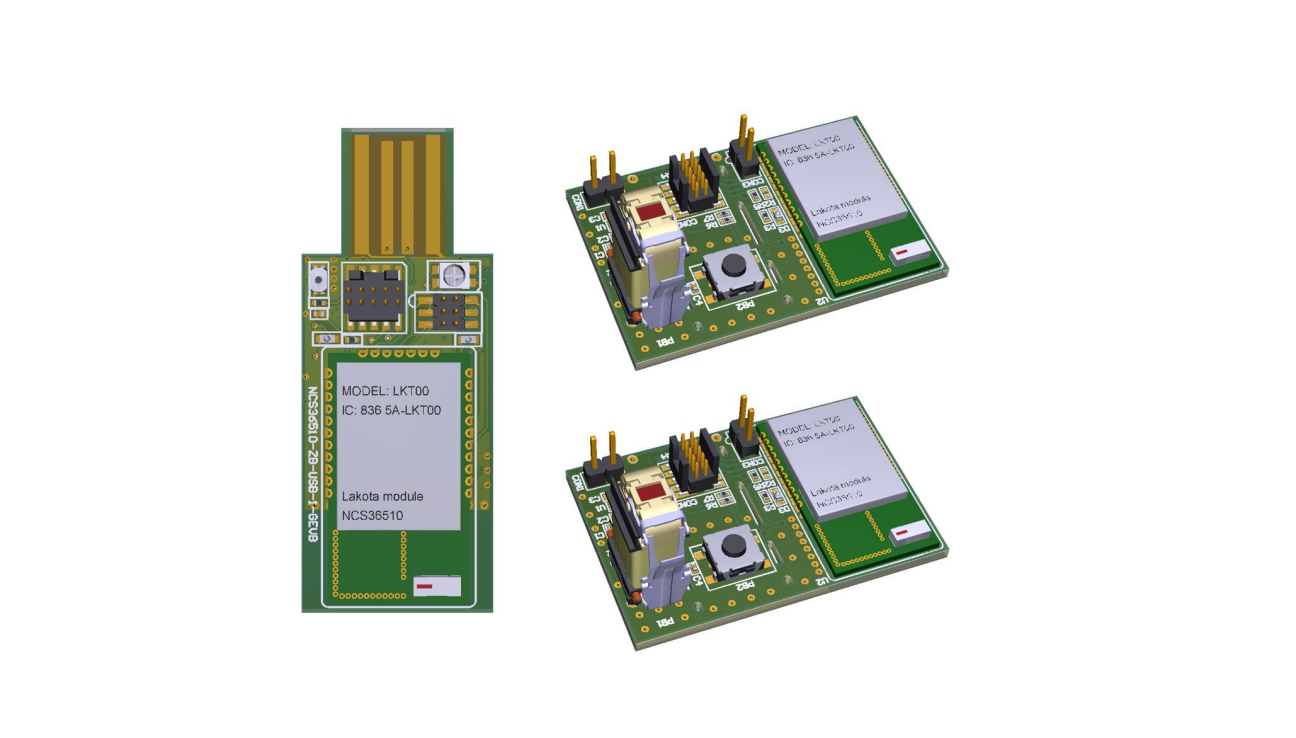
The STR-NCS36510-ZB-EH-x-GEVK is a Strata-enabled kit that demonstrates the use of NCS36510 in a battery-free Zigbee Green Power application. The kit consists of one USB device, which is the Zigbee Coordinator (ZC) and interfaces with Strata, and two energy-harvesting nodes, which act as Zigbee Green Power Devices (ZGPD). By pressing the switch on each of these devices, energy is generated and used to power the NCS36510 module. Upon booting, the module sends out Zigbee Green Power frames to control the rendered smart home scene in the Strata PC application. One switch acts as a battery-free light switch, which controls the lighting in the scene when pressed. The other switch represents a door sensor, and when pressed will open and close the door in the scene.
Figure 1: Zigbee Green Power Strata Kit Contents
Device Features
- 2.4 GHz IEEE 802.15.4 module Pre-Certified with FCC and Zigbee PRO R21
- Firmware based on the DSR ZBOSS Zigbee 3.0 & Zigbee Green Power Stacks
- 32-bit ARM Cortex−M3 Processor
- Ultra-Low Transmit Power Consumption (as low as 6.9 mW)
- Ultra-Low Receive Power Consumption (as low as 6.6 mW)
- Multiple Sleep Modes (Including 0.65 µA Coma Mode Sleep Current, 0.18 µA Coma Mode Leakage Current)
- Embedded Memory Configurations (640 kB FLASH and 48kB RAM)
- Exceptional Receiver Sensitivity of -99 dBm
- Programmable Output Power Up to ~8 dBm
Applications
- IEEE 802.15.4 Zigbee / 6LoWPAN / Thread Wireless Applications
- Smart home – Security, Automation, and Lighting
- Building and Industrial Automation
User Guide
This section provides an overview of the example application and how it functions, as well as instructions for setup and use.
System Overview
This kit consists of three boards: one USB dongle and two energy harvesting switches. The USB Dongle (NCS36510-ZBUSB-GEVB) is programmed with firmware that uses the DSR ZBOSS Zigbee 3.0 library, and is configured to be a Zigbee Coordinator (ZC). This device also interfaces with the Strata PC application via a JSON API, which is accessed via the FTDI USB-UART adapter. The Energy Harvesting Switch (NCS36510-ZB-EH-SWITCH-GEVB) is programmed with firmware to function as a Zigbee Green Power Device (ZGPD). It uses a ZF AFIG-0007 generator to provide power to the NCS36510 module via a rectifier and regulator. Each time the switch is pressed, a Zigbee Green Power “Toggle” command is sent from the ZGPD to the ZC. The Block diagram is shown below in Figure 2.
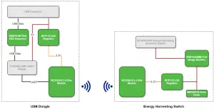 Figure 2: System Block Diagram
Figure 3 shows the correct method to press the ZF switch to activate the ZGPD device. Figure 4 illustrates the process by which the electrical current is generated. The negative voltage pulse generated by the “release” phase is rectified using the NRS1030QMU device.
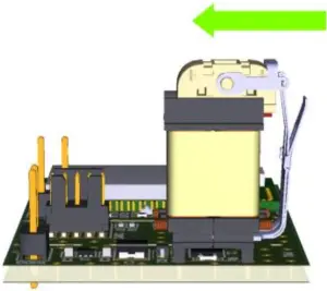 Figure 3: Operation of the ZF Energy Harvesting Switch
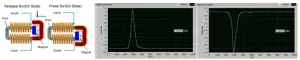 Figure 4: Energy Harvesting Power Generation
These pulses charge a 33 uF capacitor, which feeds an NCP170 LDO, which provides a 3.3V supply to the NCS36510. As the charge is consumed, the voltage gradually decreases until the NCS36510 device powers down. This results in approximately 17 ms of available “run time” for the device. The startup of the device occurs in less than 5.6 ms, and a single ZGP frame is immediately transmitted. After transmission, the ZGPD switches to receive mode to listen for an 802.15.4 ACK from the ZC. Once received, the radio is powered down and an LED is illuminated until the available power is exhausted. If no ACK is received, the ZGPD will repeat the transmission / receive cycle as many times as possible. The DC current supply and consumption waveforms are shown below in figure 5.
Figure 5: Waveforms of Regulated Supply (Yellow) and Device Current Consumption (Red)
This kit has been prepared so that each of the boards are programmed and the ZGPD nodes are commissioned with the ZC. To start this application, follow these steps:
- Download the latest version of Strata from https://www.onsemi.com/support/strata-developer-studio
- Open the Strata PC application and log in.
- Connect the USB dongle (ZC) to the computer as shown in figure 6.
 Figure 6: Hardware Setup
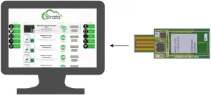 Figure 6: Hardware Setup
User Interface
Once the ZC device is connected to the PC via USB, the NCS36510 Zigbee Smart Home UI displayed in Figure 7 will appear. This window contains a rendered scene of a modern smart home, and simulates both a Zigbee 3.0 lighting system and a security sensor on the door. Clicking one switch will toggle the lights on/off, and clicking the other will render the door open or closed.
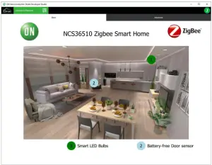 Figure 7: Main UI View
The Advanced tab displays a live feed of debug messages being sent from the Strata-enabled ZC device to Strata. This is shown in Figure 8.
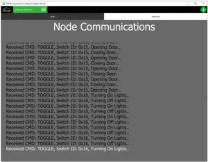 Figure 8: Advanced UI View
Programming
While these devices come programmed with the firmware for the Strata application, they can be re-programmed and used as part of custom Zigbee 3.0 application development. Please refer to the NCS36510 Zigbee SDK User Manual for additional information on setup and use of the Zigbee SDK. This is available as part of the Zigbee SDK, downloadable from the NCS36510 product page. This section details how to use the included files from the Strata content tab to restore the Zigbee Strata application onto the kit hardware.
The following items are needed:
- Strata firmware, available in the Downloads section of the Platform Content tab of Strata
- J-Link debugger, with Jlink.exe installed and included in the system PATH variable
- 3.3V DC power supply
To flash the devices, follow the steps listed below:
Zigbee Coordinator:
- Insert the board into a USB slot and connect to the J-Link as shown in Figure 9
- Open Windows command prompt, and navigate to the STR-NCS36510-ZB-EH-GEVK_firmware_images directory
- Execute the following command: “erase_nvram.bat”
- Execute the following command: “load_custom_firmware.bat./bin/light_zc_combo.bin”
- Once flashing completes successfully, disconnect the board from the PCFigure 9: J-Link connection to USB Board
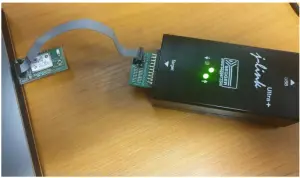 Figure 9: J-Link connection to USB Board
Zigbee Green Power Harvesting Switch
- Connect the J-Link to the board as shown in figure 10.
- Power the board with a 3.3V DC supply, as shown in figure 10.
- From the Windows Command prompt, at the same location as above, execute the following two command to update the bootloader for the ZGPD device: “load_bootloader.bat”
- For one of the ZGPD boards, run the following command to load the firmware “load_custom_firmware.bat./bin/zgpd_on_off_0x16.bin”
- Repeat for the second ZGPD board, but with the other binary: “load_custom_firmware.bat./bin/zgpd_on_off_0x16.bin”Figure 10: J-Link connection to USB Board
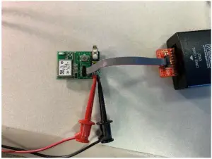 Figure 10: J-Link connection to USB Board
After programming, commission the switch nodes with the coordinator:
- Plug in the coordinator
- Wait 20 seconds for ZGPD commissioning to begin
- Click one ZGPD switch. The LED on the ZC should toggle
- Wait for the LED to change states again, indicating that the ZC is ready to add the second device
- Click the other ZGPD switch. The LED on the ZC should toggle
- The system is now ready for use with Strata
ON Semiconductor and the ON Semiconductor logo are trademarks of Semiconductor Components Industries, LLC dba ON Semiconductor or its subsidiaries in the United States and/or other countries. ON Semiconductor owns the rights to a number of patents, trademarks, copyrights, trade secrets, and other intellectual property. A listing of ON Semiconductor’s product/patent coverage may be accessed at www.onsemi.com/site/pdf/Patent−Marking.pdf. ON Semiconductor is an Equal Opportunity/Affirmative Action Employer. This literature is subject to all applicable copyright laws and is not for resale in any manner.
The evaluation board/kit (research and development board/kit) (hereinafter the “board”) is not a finished product and is as such not available for sale to consumers. The board is only intended for research, development, demonstration and evaluation purposes and should as such only be used in laboratory/development areas by persons with an engineering/technical training and familiar with the risks associated with handling electrical/mechanical components, systems and subsystems. This person assumes full responsibility/liability for proper and safe handling. Any other use, resale or redistribution for any other purpose is strictly prohibited.
The board is delivered “AS IS” and without warranty of any kind including, but not limited to, that the board is production−worthy, that the functions contained in the board will meet your requirements, or that the operation of the board will be uninterrupted or error free. ON Semiconductor expressly disclaims all warranties, express, implied or otherwise, including without limitation, warranties of fitness for a particular purpose and non−infringement of intellectual property rights.
ON Semiconductor reserves the right to make changes without further notice to any board.
You are responsible for determining whether the board will be suitable for your intended use or application or will achieve your intended results. Prior to using or distributing any systems that have been evaluated, designed or tested using the board, you agree to test and validate your design to confirm the functionality for your application. Any technical, applications or design information or advice, quality characterization, reliability data or other services provided by ON Semiconductor shall not constitute any representation or warranty by ON Semiconductor, and no additional obligations or liabilities shall arise from ON Semiconductor having provided such information or services.
The boards are not designed, intended, or authorized for use in life support systems, or any FDA Class 3 medical devices or medical devices with a similar or equivalent classification in a foreign jurisdiction, or any devices intended for implantation in the human body. Should you purchase or use the board for any such unintended or unauthorized application, you shall indemnify and hold ON Semiconductor and its officers, employees, subsidiaries, affiliates, and distributors harmless against all claims, costs, damages, and expenses, and reasonable attorney fees arising out of, directly or indirectly, any claim of personal injury or death associated with such unintended or unauthorized use, even if such claim alleges that ON Semiconductor was negligent regarding the design or manufacture of the board.
This evaluation board/kit does not fall within the scope of the European Union directives regarding electromagnetic compatibility, restricted substances (RoHS), recycling (WEEE), FCC, CE or UL, and may not meet the technical requirements of these or other related directives.
FCC WARNING – This evaluation board/kit is intended for use for engineering development, demonstration, or evaluation purposes only and is not considered by ON Semiconductor to be a finished end product fit for general consumer use. It may generate, use, or radiate radio frequency energy and has not been tested for compliance with the limits of computing devices pursuant to part 15 of FCC rules, which are designed to provide reasonable protection against radio frequency interference. Operation of this equipment may cause interference with radio communications, in which case the user shall be responsible, at its expense, to take whatever measures may be required to correct this interference.
ON Semiconductor does not convey any license under its patent rights nor the rights of others.
LIMITATIONS OF LIABILITY: ON Semiconductor shall not be liable for any special, consequential, incidental, indirect or punitive damages, including, but not limited to the costs of requalification, delay, loss of profits or goodwill, arising out of or in connection with the board, even if ON Semiconductor is advised of the possibility of such damages. In no event shall ON Semiconductor’s aggregate liability from any obligation arising out of or in connection with the board, under any theory of liability, exceed the purchase price paid for the board, if any
PUBLICATION ORDERING INFORMATION
LITERATURE FULLFILLMENT:Literature Distribution Center for ON Semiconductor 19521 E.32nd Pkwy, Aurora, Colorado 80011 USAPhone: 303−675−2175 or 800−344−3860Toll Free USA/CanadaFax: 303−675−2176 or 800−344−3867Toll Free USA/CanadaEmail: [email protected]
N. American Technical Support:800−282−9855 Toll Free USA/Canada
Europe, Middle East and Africa Technical Support:Phone: 421 33 790 2910
ON Semiconductor Website:https://www.onsemi.com/
Order Literature:https://www.onsemi.com/orderlit
For additional information, please contact your local Sales Representative
 report this ad
References
NCS36510: Low Power System-on-Chip For 2.4 GHz IEEE 802.15.4 Applications Including Zigbee®, Thread®, and Proprietary
Strata Developer Studio
Intelligent Power and Sensing Technologies | onsemi
Order Literature
Intelligent Power and Sensing Technologies | onsemi
Intelligent Power and Sensing Technologies | onsemi
[xyz-ips snippet=”download-snippet”]