
PROCEEDINGS OF SPIE
SPIEDigitalLibrary.org/conference-proceedings-of-spie
SEM AutoAnalysis for reducedturnaround time and to ensure repair quality of EUV photomasks
Kokila Egodage, Fan Tu, Horst Schneider, Christian F.Hermanns, Grizelda Kersteen, et al.
Kokila Egodage, Fan Tu, Horst Schneider, Christian F. Hermanns, Grizelda Kersteen, Bartholomaeus Szafranek, Kristian Schulz, “SEM AutoAnalysis for reduced turnaround time and to ensure repair quality of EUV photomasks,”Proc. SPIE 11147, International Conference on Extreme Ultraviolet Lithography 2019, 111471G (26 September 2019); doi: 10.1117/12.2538474 Event: SPIE Photomask Technology + EUV Lithography, 2019, Monterey, California, United States
SEM AutoAnalysis for reduced turnaround time and to ensure repair quality of EUV photomasksKokila Egodage*a, Fan Tub, Horst Schneiderb, Christian F. Hermannsb, Grizelda Kersteenc, Bartholomaeus Szafranekb, Kristian Schulz aaCarl Zeiss SMT GmbH, Carl-Zeiss-Promenade 10, 07745 Jena, Germany; bCarl Zeiss SMT GmbH, Industriestrasse 1, 64380, Rossdorf, Germany; cCarl Zeiss SMT GmbH, Rudolf-Eber-Strasse 2, 73447, Oberkochen, Germany.
ABSTRACT
With the semiconductor industry tending towards adding multiple layers consisting of EUV technology in high-end manufacturing and the production of many EUV scanners to meet customer demands, novel approaches for EUV defect review are being readily investigated. The successor of the quasi industry standard AIMS™ and sole actinic defectreview tool available currently is AIMS™ EUV. As the industry already introduced this newcomer in the manufacturing environment, other steps in the workflow were forced to adapt to the new technology. One example is the automated aerial image analysis process where the DUV aerial image analysis software, AIMS™ AutoAnalysis (AAA), was enhanced for the EUV solution in order to handle high resolution EUV images. This was a necessary step for full automation similar to the process achieved with AIMS™ and AAA.
Another important domain in the back end of line is defect repair where the e-beam based repair tool MeRiT® is also the quasi standard in the mask manufacturing industry especially for high-end photomasks. After undergoing changes to keep up with shrinking feature sizes and complex repairs MeRiT® tools were able to overcome these challenges and fulfill the current industry demands and expectations. For mask makers timely supply of error free high-quality masks is of the essence which can be further ensured by introducing a higher level of automation to the repair workflow.Following a similar approach to the optical counterpart, a digital solution known as SEM AutoAnalysis (SAA) has been developed. With SAA, a quick and fully automated SEM image-based quality assessment after a repair of a photomask is readily achievable. Moreover, the repair technicians benefit vastly by having the complete repair history of a defect for their decision-making process which would lead to a reduction of the turnaround time. As a consequence, unnecessary time wastes during mask un/loading cycles can be avoided.
The myriad data produced in the BEOL, originating from different modalities, can be converted to meaningful information with the help of automation enabling technicians to make better decisions, reducing the risk of mishaps, improve repair quality and reliability of processes in general. Since mask defects that go through each tool are the same, data produced by different tools should retain that common denominator for an efficient assessment. This assessment needs to be applied to the areas of different modalities where a comparison is possible that led to the investigations to test the feasibility of combining SEM and EUV data. A comparison of SAA results with AIMS™ EUV measurements analyzed with AAA on the same photomask and defects are presented along with this proceeding. The results show that SAA can provide a valuable preliminary assessment of photomask repairs. Nevertheless, due to the nature of SEM based analysis, AIMS™ EUV technology remains mandatory for a final mask repair qualification and a complete specification check, i.e. mask repair verification. The outcome of this investigation paves the way towards a fully automated BEOL where different workflows and data originating from several tools in the mask shop can be interconnected and controlled.
Keywords: SEM AutoAnalysis, AIMS™ AutoAnalysis, EUV, SEM, aerial image, MeRiT®, AIMS™
INTRODUCTION
Since the introduction of EUV in the semiconductor industry most of the major players have been gradually incorporating changes to their already well-established processes in mask shops to accommodate the newcomer. Within the past few years major investigations were carried out to find the most appropriate EUV blanks as well as pellicle material. Currently these investigations are being continued to achieve better line edge/width roughness, reduced numberof defects and durable/sustainable photomasks [1, 2]. Furthermore, multi-patterning appears promising as it brings sub- 50nm features onto masks [3]. As a result, tighter specifications are applied that essentially increases the number of defects on reticles. Keeping the latter at bay is vital because a single particle can have negative repercussions in terms of the wafer yield [4]. Therefore, the defect review sector in the BEOL welcomed the AIMS™ EUV tool that successfully captures high resolution images compensating for the decreasing feature sizes. This forced mask makers to make necessary adjustments in the mask shops emphasizing its importance for production.
Reflecting upon this experience, mask shops would have to optimize processes in the BEOL to quickly adapt to changes and customer demands. Using smart automation especially when faced with smaller specifications and increasing number of defects, would be one way to adapt to changing conditions. The need for such a solution is seen by thepersistently high turnaround time (TAT) at smaller nodes in the past couple of years [5]. The complexity of masks also worsens the situation as the sub-resolution assist features (SRAFs) would reduce to 32-40 nm [6]. Considering the current working scenario in the BEOL even having a handful of defects on the mask can mean many un/loading cyclesbefore the mask is defect free. To combat this trend, an industry proven solution offers the use of data-connectivity and automation in a well-designed architecture that is both flexible and stable. It utilizes a software known as AIMS™ AutoAnalysis (AAA) that carries out automated defect analysis and produces a comprehensive report with desired level of detail [7]. Direct connection with the AIMS™ tool via the FAVOR® system enables parallel defect analysis once both aerial reference and defect images are available. This not only minimizes operator involvement avoiding any mishaps but also allows the flexibility to view analyzed data directly after measurements. The application works in a modular fashion that enables changes quicker than in any other arrangement. For example, the internal working segments of the software such as analysis recipes and report templates can be easily modified and attached to specific analysis jobs that would function untouched until needed. As expected the inclusion of AAA in the BEOL has reduced the time taken during the repair-review cycles, reduced misclassifications and enabled a comprehensive analysis of defects and repairs [7]. Similarly, EUV defect review benefits from this software solution that would keep the TAT from exploding. AAA hasundergone changes to adapt to specific EUV applications i.e. the ability to cope with large data traffic produced by the high-resolution aerial images captured by the AIMS™ EUV tool. Such capability promotes smaller yet different defect types to be spotted at a quicker pace without wasting operator time.
The defects that occur on EUV masks are clearly different to that encountered with that of DUV due to the multilayer structure of the former. The defect types range from phase defects, translated from the substrate through the multilayer, to regular hard defects which occur during fabrication [1, 2]. Contamination can always occur during any application step and these repairs strongly impose on-time tool adaptability. The MeRiT® tool has overcome this challenge and successfully displays the capability to repair EUV defects taking the lead in this domain. To extend the level of automation from defect review to repair, single MeRiT® tool preparation steps have been automated that essentially frees the operator to carry out other tasks while the processes run. Following the footsteps of the aerial domain implementation, the software SEM AutoAnalysis (SAA) enables the automatic analysis of defects and post-repairs after each image acquisition. Initially, steps to customize analysis recipes and report templates must be carried out for each feature type but after the initial time investment the prepared modular components can be readily used for later jobs. This would save a lot of time in the long run. SAA gives the operator a detailed overview of the defects that can be compared against the specifications and assists in arriving to a decision regarding the type of defect and the subsequent effects on the mask. The operator is provided with tangible results to assist in realizing the kind of repair and defect severity. Compared to the aerial version, completely different algorithms are used for SEM image processing given the native differences between the two image types. Furthermore, analysis strategies have been specially modified and designed to fit the use cases which will be mentioned in the methodology.
SAA in combination with the repair tool MeRiT® brings many advantages to mask shops. The feature in MeRiT®, known as SEM Review, together with SAA can in fact replace long term costs of maintaining a separate tool for bulk defect capture as it enables automated imaging of defects including navigation and autofocus. Intermediate steps until the repair can also be implemented elsewhere freeing the tool for more measurements. Uncomplicated repairs can be carried out automatically with the option for manual intervention whenever needed via the MeRiT® feature Advanced AutoRepair.This leads to improved repair quality and process reliability in the repair regime. The fact that SAA is able to use images that are automatically grabbed by the tool during repair makes it easy for the user rather than capturing extra images for a third-party software.
For a complete assessment of repairs, data from more than one modality is always useful since they assist in making better decisions. Taking mask defects into account, the repair and review processes contain the common aspect that their local coordinates are identical even though imaged through two different modalities. Currently data from these two modalities are handled separately that would lead to ~35% of time being wasted compared to that with repair optimization and disposition automation [8]. There are measures taken via machine learning to close this gap, for example, by using one image type as input and predicting the other but these studies are still in the research phase and not ready for high-volume manufacture [9, 10].
Focusing on the repair verification loop, the data commonly used are SEM and aerial images. As a first step towards the accurate alignment of both EUV and SEM images systematic investigations were conducted where both AAA EUV and SAA were used for image analysis, respectively. This led to a comparison between the two types of data. Both lines and spaces and contact hole images were captured using a ZEIS internal mask. Given the nature of both modalities the conditions for assessment were varied as thought fit. These are the preliminary steps in the BEOL towards a fully connected mask shop that leverages the vast amount of data produced automatically on a daily basis.
1.1 Comparing Aerial and SEM imaging
Similar to all imaging methods aerial and SEM imaging both have dedicated tools with preparation/calibration steps that are very different to one another. If these tool preparation steps are not followed accurately the images can have undesirable side effects. The AIMS™ tool was mainly developed to detect defects and all related processes are optimized to reflect the final wafer printability. The four times magnification from wafer to mask causes errors, present on masks, to be transferred to wafer and this ratio, known as mask error enhancement factor (MEEF), leads to defects that are larger on wafers than on masks. This ratio is small for EUVL compared to that of 193i [11]. This behavior however does not persist in SEM images since imaging is carried out one-to-one at the mask as the MeRiT® tool was initially developed for repair or defect review purposes. Therefore, estimating printability is difficult only using SEM images, other than developing other methods include simulations.
In terms of detecting phase defects aerial imaging is at the forefront. With the help of Bossung plots through-focus variations can be readily identified [12]. On the contrary, phase defects are not visible on SEM images as the secondary electrons, generated during the interaction of the primary beam and the substrate, can produce the same intensity in the defect and the unaffected areas. This difference between the two modalities is simply due to the principles of the imaging tools. Another aspect, as a result, is that the SEM images magnify roughness information compared to that with aerial. Due to the high resolution of SEM images, more information of the line width roughness is captured which can be used for further detailed analysis of the mask. The resolution of AIMS™ EUV is at its best for an optical system. As published by Chen et al. the line width roughness between AIMS™ EUV and SEM resists behave as similarly [13]. This leads to the conclusion that SEM defect detection can be considered as an inspection tool that detects very many variations that can be later be filtered. Especially with the lack of inspection tools for EUVL, defect detecting methods using SEM images is an asset to the BEOL.
METHODOLOGY
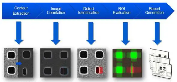
Since two completely different modalities are being compared, i.e. SEM and aerial, the test implementations were aligned and adjusted with one another. As for our image data set two feature types were investigated i.e. periodic lines and spaces patterns and periodic contact hole patterns. For defect identification a reference image with no defects is required to compare with the defect image. The only restriction on the software is that the image sizes should be the same. There are various contour extraction algorithms available that fit to different mask/feature types and the contour extraction parameters can be manually edited to obtain perfect contours. This is the heart of the software as all the following steps depend on the contour extraction. Another feature that is applicable for post repair images is the cropping function enabling the software to only focus on a specific region. As post repair SEM images contain DC dots that can be falsely detected as a defect the above function is very useful. Then both reference and defect images are correlated followed by the defect identification step. Furthermore, a more detailed analysis is conducted depending on the criteria given on the analysis recipe. Finally, a comprehensive report can be produced with user defined filters to emphasize desirable data. All the above steps of the SAA software workflow are depicted in Figure 1.
Images captured must also be suitable in terms of quality. The MeRiT® captures images with sufficient resolution and good quality with respect to noise levels, contrast and roughness. This is the same for AIMS™ EUV tool and the image analysis workflow in AAA which is the same as described for SAA.
Lines and Spaces patterns
In total 12 image pairs were analyzed of which 10 are 68nm half pitch lines and spaces and contained 7 nm extrusion defects (please note, that all dimensions are on mask level). Moreover, post repair images of a 68 nm single and a triple bridge with a length of 1000 nm along with relevant reference images for both SAA and AAA were considered. Theimages were 4500 × 4500 nm2 with a resolution of 3000 × 3000 pixels and the post repair SEM images contain DC dots.
First, the behavior of CDs between the two modalities were investigated. A larger area on SEM images, 1898 × 1489 nm2, was chosen due to the larger line edge/width roughness compared to aerial images, 1194 × 411 nm2. These results were used for an initial analysis of the approximate range of the CD values in the SEM and aerial images.
Then, the line-line comparison produced a more detailed investigation. Figure 2 shows an image set showing the raw SEM image with a 7 nm programed extrusion defect (left). Note: the center line is slightly wider than the neighbor lines.After processing with SAA, a contour extracted image overlaid with CD variations can be obtained (middle). The color coding represents failing (red) and critical (orange) regions. This categorization can be customized in the analysis recipe and for this case the failing regions represent > ±10 % and critical regions > ±8 % CD deviations. The aerial image on the right is the variant of SEM but only shows pass and fail regions for simplicity.
Contact Hole patterns
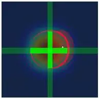
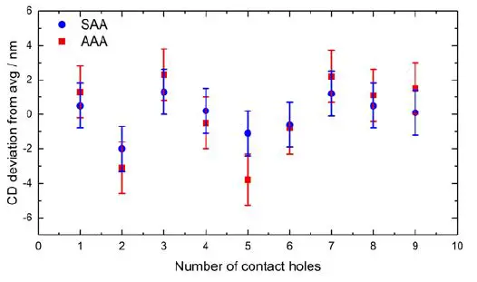
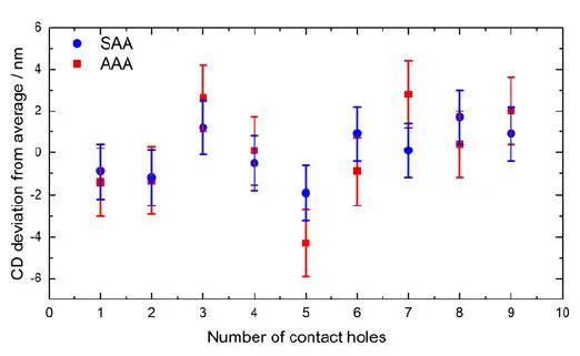
For the contact hole data set 6 image pairs were considered. The contact holes were 140 nm in edge length and each image was 3000 × 3000 pixels. The distance between each contact hole in X and Y is 200 nm (outer edge- outer edge). The defect types were varying: 1 missing and 5 half missing contact holes. Figure 3 displays a sequence of images that represent the analysis criteria possible with contact holes. Besides the CD widths, the area of the reference and defect contact holes can be compared. In addition, the placement of the contact holes at specified angles can be evaluated with respect to the reference image. Figure 3 D shows this clearly as the placement is calculated at 0, 45 and 90 degrees.
Due to the difference in optical resolution of the AIMS™ EUV the contact holes seem rounder than that on SEM images. With the help of the analysis recipe only a narrow region was used for analysis (Fig 3. B and Fig 4.), both vertically and horizontally (Fig 4.). Of course, more directions are possible, but we took only two directions for simplicity. AAA/ SAA automatically detects any area deviation when analyzing contact holes and this is depicted with the red blob in Figure 4. The slices do not show any defect since the horizontal CD width comparison results in a pass with respect to the applied tolerance criteria.
RESULTS AND DISCUSSION
During the investigations the measurement metric was varied between SEM and aerial images mainly to compensate for the natural difference in the two image types. Especially with SEM images that captured more rugged topological information, post processing steps such as smoothing and alignment of plots in x- and y-axis were applied when necessary. Figure 5 shows the raw SEM CD values across a 68 nm single bridge post repair which is far more volatile compared to AIMS™ EUV data shown in Figure 8 (red).
Lines and Spaces patterns
Given the large line width roughness in SEM images, a larger area on the SEM image was considered for an initial comparison. This resulted in an interesting trend where the CDs from the aerial image was well nested within the values extracted from the SEM image. Figure 6 displays the CD widths of three neighboring lines on AIMS™ EUV and SEMimages. The CD widths were extracted using both AAA and SAA, respectively. The SEM CD widths are within the standard deviation of AIMS™ EUV values.
The discrepancy between the two values relates to the differences mentioned in section 1.1. which leads to the conclusion that SAA can detect more variations.
When comparing CD deviations observed in SEM and AIMS™ EUV images a similar trend surfaced. Average CDs of the repaired area in the post-repair image were compared with the average reference CDs. Taking the average specially for SEM images enabled to have a more comparable statistics and minimized the effects of the high line edge/width roughness (Figure 7).
CD widths extracted from SEM and aerial images proved the above observation further. The results from SAA (blue) shown in Figure 8 and 9 are processed using a smoothing filter to be able to compare with the aerial images. This compensates for the native roughness levels of SEM images. Vertical and lateral adjustments to the plots were necessary for clarity and adjust for the differnce stage alignment between two tools. Figure 8 shows the comparison of a 68 nm single bridge defect after repair whereas Figure 9 is that of a 68 nm triple birdge defect.
Smaller scale analysis, i.e. only considering single lines and CD widths, shows similar variations between both modalities even though expectedly raw SEM plots show more peaks compared to that in aerial images (Fig 5.). The peaks align considerably well between SAA and AAA results. However, the variability between the two is quite large and this matching depends on the quality of the repair. With the triple bridge example, it can be seen that a repair taking place in close vicinity could affect the variability of SEM data. However, SAA and AAA data show similarities between -600 – 400 nm and 200 – 400 nm.
Contact hole patterns
Both vertical and horizontal CDs were measured with the focus on one simple post-repair defect where the middle contact hole was missing. The contact holes surrounding this etch were also analyzed and all data are plotted in Figures 10 and 11. The CD deviation from average was compared between both SAA and AAA results. For better comparison between the two images the threshold of AIMS™ EUV results was increased by 16.7%. This allowed to take the average CD deviation in both cases and the tolerance criteria were kept the same for both modalities i.e. at >±8% fail and >±5% critical. AAA had identified a defect at the right edge of the repaired contact hole (Fig. 4) due to the differences in area between reference and post-repair images even though the result status was labelled pass, whereas critical for SAA.
SUMMARY AND OUTLOOK
For the efficient reduction of TAT in the back-end of mask manufacturing many time-consuming intermediate steps, such as queueing, loading and unloading masks and shuttle time, between MeRiT® and AIMS™ EUV systems were addressed by comparing their SEM and aerial images, respectively. The results show that the CD widths as well as CD deviation measurements follow a similar trend with SEM and AIMS™ EUV images. The entire analysis was carried out via the software SAA and AAA, respectively. Despite using different analysis algorithms, the trends were visible. This leads to the conclusion that SAA data is not an exact match to that of AAA but comparable and demonstrates a similar trend. Industry in fact needs AIMS™ EUV for flawless defect disposition and verification.
If such an implementation were to enter mask shops, an all-inclusive data connectivity is achievable. Having access to complete data sets that the MeRiT® and AIMS™ EUV tools produce, these preliminary efforts can be further improved to a product that shows a relative verification after a defect repair. This enables technicians to make quicker and reliable decisions when estimating the quality of a repaired defect. Moreover, with the lack of an actinic pattern mask inspection tool for EUVL, SEM images are a great resource. AIMS™ EUV being bulky and expensive, though the gold standard of defect verification, this implementation is seen as a bridging technology until the EUV verification tool reaches the mask shops.
Besides the comparable analysis results of SAA and AAA, both applications provide an automated way of evaluating SEM and aerial images within a short time and an improved reliability in comparison to even experienced operators [7]. To further extend the degree of automation with all its benefits as well as the correlation to other tools and data types, a similar investigation as presented here is necessary. All captured data can then be collected and viewed on the overarching solution, Advanced Repair Center (ARC), which further enhances the efficiency and reliability of mask shops.
ACKNOWLEDGEMENTS
We would like to thank Dr. Dmitry Simakov, Dr. Renzo Capelli, Dr. Michael Waldow and Matthias Stecher for fruitful discussions.
REFERENCES
- Rastegar, A., Jindal, V., “EUV mask defects and their removal”, Proc. SPIE 8352, 83520W (2012).
- Huh, S., Ren, L., Chan, D., Wurm, S., Goldberg, K., Mochi, I., Nakajima, T., Kishimoto, M., Ahn, B., Kang, I., Park, J., Cho, K., Han, S., Laursen, T., “A study of defects on EUV masks using blank inspection, patterned mask inspection, and wafer inspection”, Proc. SPIE 7636, 76360K (2010).
- Simone, D. D., Singh, A., Vandenberghe, G., “Printability study of EUV double patterning for CMOS metal layers”, Proc. SPIE 10957, 109570Q (2019).
- LePedus, “EUV mask gaps and issues”, Semiconductor Engineering, 8 May 2019,https://semiengineering.com/euv-mask-gaps-and-issues/ (4 July 2019)
- eBeam Initiative, “Mask Maker Survey”, 18 September 2018, https://www.ebeam.org/docs/eBe.am-Mask-Maker-Survey-2018.pdf (24 July 2019).
- LaPedus M., “More EUV mask gaps”, Semiconductor Engineering, 17 November 2016, https://semiengineering.com/more-euv-mask-gaps/ (25 July 2019).
- Russell, G., Jenkins, D., Goonesekera, A., Dornbusch, K., Sargsyan, V., Zachmann, H., Buttgereit, U., “Automated defect disposition with AIMS AutoAnalysis”, Proc. SPIE 10451, Photomask Technology, 1045113 (2017).
- Schulz, K., Egodage, K., Tabbone, G., Garetto, A., “How smart is your BEOL? productivity improvement through intelligent automation,” Proc. SPIE 10454, 104540X, (2017).
- Bürgel, C., Sczyra, M., Utzny, C., “Necessity is the mother of invention: support vector machines for CD control”, EMLC Dresden, VDE, (2019).
- Evanschitzky, P., “Mask defect assessment from SEM images aided by deep learning methods”, EMLC Dresden,VDE, (2019).
- Walia S., [Low Power Semiconductor Devices and Processes for Emerging Applications in Communications, Computing and Sensing] CRC Press, Boca Raton, 5-6, (2019)
- Garetto, A., Uzzel, D., Magnusson, K., Morgan, J., Tabbone, G., “Utilization of AIMS Bossung plots to predict Qz height deviations from nominal,” Proc. SPIE 8886, 88860K (2013).
- Chen, X., Verduijn, V., Wood, O., Brunner, T., Capelli, R., Hellweg, D., Dietzel, M., Kersteen, G., “Evaluation of EUV mask impacts on wafer line-edge roughness using aerial and SEM image analyses,” Proc. SPIE 10583, 105830J (2018)
Spie SEM Auto Analysis for reduced turnaround time and to ensure repair quality of EUV Photomasks Instruction Manual – Spie SEM Auto Analysis for reduced turnaround time and to ensure repair quality of EUV Photomasks Instruction Manual –
[xyz-ips snippet=”download-snippet”]